
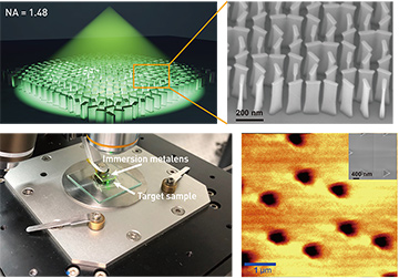
 Top: Sketch of the immersion metalens with ultra-high numerical aperture (left), with SEM micrograph detail (right) showing the high aspect ratio of each crystalline silicon nanobrick. Bottom: Scanning confocal microscope using the oil immersion metalens for imaging (left), and image of a target sample obtained with the immersion metalens in scanning mode (right). Inset shows an SEM image of the target sample, which consists of silicon triangles on a glass substrate. [Enlarge figure]
Metalenses focus light using subwavelength artificial nanostructures. Such ultra-thin lenses, made with titanium dioxide, gallium nitride, and silicon nitride, have already exhibited impressive optical performance in the visible regime, with a lack of spherical aberration and near-unity numerical aperture (NA).1,2 Obtaining NA values higher than 1, however, requires immersion liquids to increase the background refractive index—and, at this point, metalenses lose their ability to focus light due to the reduced index contrast.3 How can metalenses achieve ultra-high NA?
In 2017, we introduced crystalline silicon as a promising material for metalenses, even in the visible regime, and demonstrated high NA and high transmission.4 We implemented a geometrical-phase approach, with “nanobricks” arranged in a spherical-aberration-free phase profile, and designed a metalens with NA = 0.98 in air. Due to the high refractive index of the crystalline silicon, this metalens can be further front-immersed into immersion oil to achieve an ultrahigh NA of 1.48 experimentally and 1.73 theoretically on a sapphire substrate—the highest NA in the visible regime ever reported for a metalens.5
Our work highlights several exciting aspects of metalenses. These lenses can achieve diffraction-limited operation even for an ultra-high NA of 1.48; can perform competitively compared with conventional objective lenses in the scanning imaging mode; and can be made in silicon, so they are CMOS compatible. Using a hybrid optimization algorithm for the design, with a target function that emphasizes both phase fidelity and high transmission, we have also shown that the best crystalline silicon nanobrick arrangement can reach high transmission values comparable to those made in dielectric materials such as titanium dioxide. The work thus validates sophisticated computational optimization as an effective tool for nanostructure design.
We envision that this design will push metasurfaces into practical applications such as high-resolution, low-cost confocal microscopy and achromatic lenses.
Researchers
Haowen Liang, Juntao Li, Jianying Zhou, Sun Yat-sen University, Guangzhou, China
Xiangsheng Xie, Shantou University, Shantou, China
Thomas F. Krauss, University of York, York, U.K.
References
1. M. Khorasaninejad et al. Science 352, 1190 (2016).
2. S. Wang et al. Nat. Nanotech. 13, 227 (2018).
3. W.T. Chen et al. Nano Lett. 17, 3188 (2017).
4. Z. Zhou et al. ACS Photon. 4, 544 (2017).
5. H. Liang et al. Nano Lett. 18, 4460 (2018).
