
Conventional nanoscale imaging is difficult to perform for large, micron-scale samples due to drifts caused by thermal effects and vibrations. Researchers address this issue with a newly developed imaging system that compensates for such drifts. [Image: P. Verma, Osaka University] [Enlarge image]
Tip-enhanced Raman spectroscopy (TERS), a technique for gathering images of surfaces at nanoscale resolution, has become a useful tool for scientists who study surface defects of inorganic materials as well as single biological molecules. However, attempts to scan a large-scale surface with TERS run into a problem: after a half-hour’s work under ambient laboratory conditions, thermal and vibrational fluctuations make the system drift out of focus.
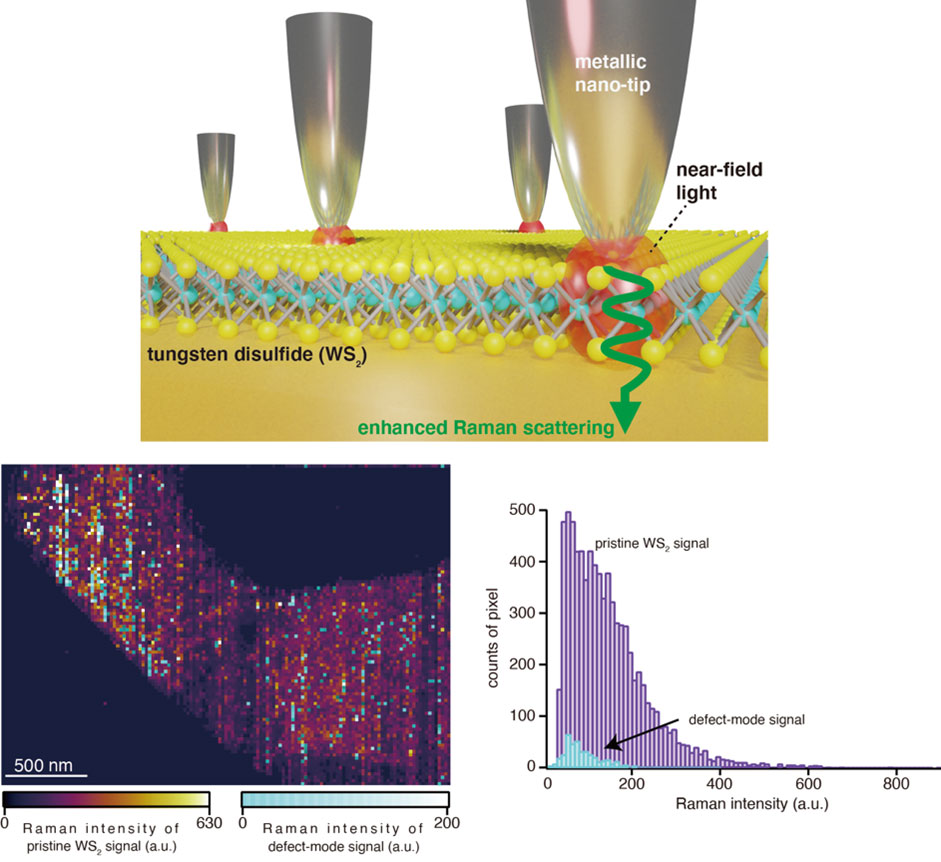
Researchers at two Japanese universities recently demonstrated long-duration TERS imaging—up to six hours, or 12 times the length of previous efforts—of a dichalcogenide crystal used in optoelectronic devices (Sci. Adv., doi: 10.1126/sciadv.abo4021). Guided by a positional sensor and feedback loop, the team’s imaging system detected both surface defects and optical signals related to the defects.
Getting ready to scale up
TERS combines a laser-based Raman microscope with either an atomic force microscope or scanning tunneling microscope. The tip “steps” over the surface of the target sample in tiny increments, often as small as 10 nm, and records images at each step.
Gathering enough scattered light to register an image takes at least a few hundred milliseconds at each step, so a TERS image of 1 μm2 takes about 30 minutes to collect. During that time, the scanning tip drifts out of its horizontal position and the optics drift out of focus in the vertical direction, degrading the signal and ending the imaging process.
According to Optica Fellow Prabhat Verma, professor of applied physics at Osaka University, Japan, TERS has reached the stage of maturity where it could be used for commercial applications, such as inspecting photonic chips—except that the inevitable drift under ambient conditions restricts the size of the surface that can be analyzed.
Feedback for better focus
Verma and his colleagues at Osaka University and Tokushima University, Japan, devised a method to compensate for the tip drift in all three dimensions. Their custom system incorporated a 488-nm guide laser and a lateral positional sensor to correct the focus. The signal traveled through a closed-loop piezo scanner, which was coupled to the objective lens to stabilize the position of the laser’s focus. To handle the tip drift, the researchers used galvanometer mirrors to scan the laser spot around the tip and produce a Rayleigh-scattering image, also used in the feedback loop to stabilize the tip position.
Verma says that the construction of the drift-compensation system was the group’s biggest challenge, which the researchers overcame by using the skills and experience gained from years of working with TERS.
The team chose tungsten disulfide on a gold substrate for the test samples for the TERS platform because the dichalcogenide has become popular in optoelectronic device research, Verma says. He added that he’s confident that the ultrastable TERS method will work for other samples in materials science and biology. He also says that the time window for TERS imaging can be extended past six hours, allowing the method to focus on samples that yield extremely weak optical signals.
