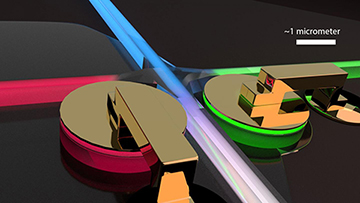
An artist’s rendering of the nanoscale opto-electro-mechanical switch recently demonstrated by a team of scientists from ETH Zurich, NIST and Chalmers University. [Image: S. Kelley/NIST]
A lightning-fast electro-opto-mechanical switch developed by a team of researchers in Switzerland, the United States and Sweden reportedly could substantially advance a number of emerging optics- and photonics-based technologies, including autonomous vehicles, neural networks, and optical and quantum computing (Science, doi: 10.1126/science.aay8645).
The new switch—operating at a speed of tens of nanoseconds—relies on an electrostatic, nanometer-scale manipulation of a thin, low-mass gold membrane that forms an air-gap hybrid photonic–plasmonic waveguide. The switch is capable of routing light from one silicon-based computer chip to another with low signal loss and at low voltages.
That ability to rapidly re-route light signals, the researchers believe, could have application in autonomous vehicles, for example, because the signals could continuously scan all parts of the roadway measuring distances between other vehicles and pedestrians. For neural networks, powerful light-based circuits could carry more information at speeds much greater than electricity-based circuits, aiding such tasks as pattern recognition and risk management.
Photonic–plasmonic marriage
The switch exploits the wave nature of incoming light. Electrostatic adjustment of its gold membrane creates light waves that either interfere constructively, aligning and reinforcing each other, or destructively, cresting out of step and canceling each other.
With destructive interference, the research team reports, the switch can redirect light to another chip with low signal loss. Also important, light leaking from the chip’s silicon waveguide strikes the gold membrane, inducing groups of electrons to oscillate as plasmons. Researchers can manipulate the plasmons over nanoscale distances—much shorter than the wavelength of the original light—before converting them back into light. This keeps the optical switch extremely compact.

Light travels along a silicon waveguide where electrostatic adjustment of a gold membrane can either block or redirect the light along a parallel waveguide to another chip with low signal loss. Plasmonic effects on the gold membrane mean the light can be manipulated over nanoscale distances, keeping chip size extremely compact. [Image: S. Kelly/NIST]
“The main advantage of our switch is the ability to induce a pi-phase shift at low driving voltage and small device size,” says project leader Christian Haffner of the National Institute of Standards and Technology and the University of Maryland, USA, and ETH Zurich, Switzerland. “Also, I am excited that we can do this with plasmonic elements without suffering from high optical losses that are normally inherent to this technology.”
Scientists once thought a plasmonic system would attenuate light signals because photons would penetrate the interior of the gold membrane where electrons would absorb much of the light energy. The compactness of the research team’s device, with a design that ensures few photons penetrate the membrane, has meant a light-signal loss of just 2.5% compared with 60% for previous optical switches. This puts the new switch within reach of commercial application, the researchers say.
What’s more, the international team hopes to make the device even smaller by shortening the distance between the gold membrane and the silicon disk, further reducing signal loss.
Toward more complex quantum circuits?
For analog computing, the ability of the new opto-mechanical switch to route high-speed optical data streams might find more immediate use in supercomputers, Haffner says. But it provides great potential for optical computing including one day optical quantum computing.
“Current optical quantum technologies—including the vision of realizing an optical quantum computer—are in need of classical phase-shifting elements that are compact and feature low energy consumption,” Haffner says. Prior-art optical switches, he notes, suffer from large energy consumption, are bulky and the heat they produce can reduce the purity of the quantum state.
“Implementing our switches in these applications could overcome these limitations enabling quantum circuits of larger complexity,” Haffner says.

