
[Image: AIM Photonics, courtesy of NIST]
The US National Institute of Standards and Technology (NIST) announced that it had entered into a cooperative agreement with the photonics public–private partnership AIM Photonics to provide improved approaches for calibrating, measuring and testing photonic integrated circuits (PICs). In a press release accompanying the announcement, NIST maintained that the R&D agreement would result in “a critical new tool” for developers of hybrid electronic-optical chips for use in communications, high-performance computing and a range of other advanced technologies.
Building a PIC research ecosystem
AIM Photonics—or, more formally, the American Institute for Manufacturing Integrated Photonics—was formed in 2015 as a result of call for proposals from the US Department of Defense for a “manufacturing innovation institute” to advance PIC development in the United States. It is one of 16 institutes under the umbrella of Manufacturing USA (formerly the National Network for Manufacturing Innovation), established in 2014 to “bring together industry, academia and federal partners” to build US infrastructure and boost US competitiveness in a range of areas tied to advanced manufacturing.
Within that broad umbrella group, the New York–based AIM Photonics focuses on maintaining an R&D ecosystem for small and mid-sized businesses, academic labs and government researchers. In that role, it provides access to “state-of-the-art integrated-photonics fabrication, packaging and testing facilities and services,” as well as developing tools, process-design kits and other supporting materials and working to foster a sustainable workforce for integrated photonics. The institute is administered by the Research Foundation for the State University of New York.
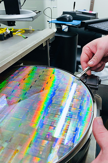
“Calibration structures” to accelerate PIC development
The NIST–AIM Photonics partnership will center on streamlining the calibration and testing of PICs. In particular, NIST—building on its experience with modeling, measuring and calibrating performance for electronic chips—will design “calibration structures” for similar measurement and testing of the electronic performance of photonic chips.
The calibration structures will be able to measure photonic-chip performance at speeds of up to 110 GHz, versus the 25-GHz speeds more typical of the current generation of photonic chips, according to NIST. Thus, NIST says, these structures should “result in improved designs” and “accelerate the development of photonic chips faster than today’s.”
The calibration structures will be able to measure photonic-chip performance at speeds of up to 110 GHz, versus the 25-GHz speeds more typical of the current generation of photonic chips, according to NIST.
AIM Photonics, for its part, will fold the new calibration structures into its foundry processes and process-design kit for PIC developers. The new structures should be available to users in roughly a year, according to the NIST release. David Harame, the chief operating officer of AIM Photonics, maintained that the enhancements would “give our members and customers the tools they need to design the next generation of advanced photonic chips.”
Chipping away
Inevitably, the unveiling of the cooperative arrangement was accompanied by allusions to the recently passed CHIPS and Science Act in the US (although the joint NIST–AIM Photonics effort was started before that statute’s passage). Under Secretary of Commerce for Standards and Technology and NIST Director Laurie E. Locascio said that the partnership “shows how government and industry can work together to drive innovation and restore U.S. global leadership in semiconductor manufacturing.”
