
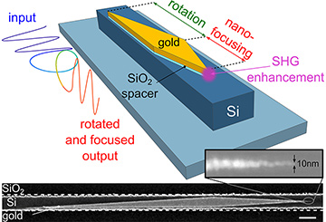
 Top: Schematic industry-standard waveguide, followed by two hybrid plasmonic circuit modules. The first leads to efficient photonic-to-plasmonic rotation (green); the second leads to nanofocusing (red). The nanofocused apex brings about second-harmonic generation at the gold nanotip (purple). Bottom: SEM top view of a fabricated device, revealing the 10-nm apex sharpness. Scale bar: 400 nm. [Enlarge figure]
Chip-based nanophotonic devices owe their success to the maturity of the fabrication technologies that enable their mass-production, but also to the modularity of their constituent components—such as gratings, splitters and couplers. These make large-scale, complex designs accessible, efficient and cost-effective.1
Plasmonic devices incorporating metals, on the other hand, enable extreme photonic miniaturization and extreme light–matter interactions, orders of magnitude better than their dielectric counterparts both in compactness and light confinement. Yet their integration with conventional photonic circuits has proved challenging, and most chip-based plasmonic functionalities have been ad hoc, ab initio designs tailored to a specific need.2 In work that was published this year, we offered an approach for hybrid silicon–plasmonic devices that enables modular design of the plasmonic elements.3
The reason for the difficulty of integrating plasmonic devices lies in their use of metals, which are lossy. Much of the light is absorbed after a few wavelengths of propagation, which limits multi-element designs. Hybrid plasmonics, which judiciously combines metals and dielectrics, mitigates these limitations by achieving photonic miniaturization at the nanoscale while minimizing losses. Nonetheless, most designs thus far have still only addressed one photonic function at a time. A modular approach to plasmonics—one that allows the assembly of different metal components onto an existing chip to enhance its functionality—has been largely absent.
We showed this year that two distinct plasmonic components, formed by hybrid plasmonic silica/gold nanolayer structures, can be post-processed on a standard near-infrared silicon photonic waveguide.3 The first plasmonic element efficiently rotates the incoming polarization in only a few wavelengths; the second component focuses the incoming light to deep subwavelength mode volumes.
In the process, we have shown strongly enhanced second-harmonic generation at the gold nanotip, which has an apex of approximately 10 nm. This experiment has allowed us to estimate that the light intensity at the nanotip is enhanced by more than 100 times relative to an equivalent gold strip. These three functionalities—plasmonic rotation, nanofocusing and nonlinear enhancement—all occur over a length of less than 10 µm of light propagation, unachievable by a conventional dielectric waveguide.
This technology has applications in chip-based nanospectroscopy, nonlinear and atomic-scale sensing, nano-interconnects, and nanoscale terahertz sources and detectors. Our modular approach fundamentally makes hybrid plasmonic technologies much more accessible.
Researchers
Alessandro Tuniz, Stefano Palomba and C. Martijn de Sterke, The University of Sydney, Sydney, Australia
References
1. L. Chrostowski and M. Hochberg. Silicon Photonics Design: From Devices to Systems (Cambridge Univ. Press, 2015).
2. F.J. Rodríguez-Fortuño et al. J. Optics 18, 123001 (2016).
3. A. Tuniz et al. Nat. Commun. 11, 2413 (2020).
