
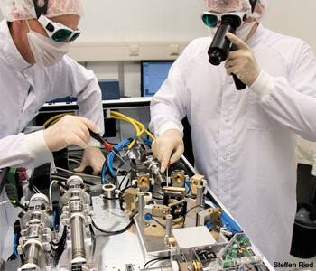
 Christoph Tillkorn and Stephan G. Strohmaier working on the wavelength combiner of a TruDiode 4006.
Laser diodes are everywhere these days. Diode beam sources have been seamlessly integrated into consumer electronics, medical equipment and many other applications. Recently, they have emerged as powerful beam sources that are capable of delivering kilowatts of power. Diodes are being used to directly process materials, such as to weld sheet metal and solder plastics.
Historically, welding applications have relied on lamp-pumped solid-state lasers. During the past few years, however, such lasers have been widely replaced by diode-pumped solid-state lasers that include fibers and thin discs as laser active media. It has always been a dream to use direct-diode lasers, which convert electrical current at very high efficiency into laser light, thereby avoiding the detour of having to rely on a fiber or disc. The evolution of lasing will surely enable very compact, efficient and robust laser systems.
Previously, the poor beam quality and low power of diode lasers have prevented them from being used successfully as direct-diode lasers in high-brilliance applications. Now, however, diode lasers are capable of achieving the high brilliance needed for deep-penetration welding, with beam qualities around 30 mm*mrad and powers in the multi-kW range. Even further on the horizon, we expect that brilliance levels suitable for high-speed cutting will be achievable with direct-diode lasers.
The broad-area edge emitter
The advances in laser-diode technology that have enabled direct welding applications have been driven by increases in the power-per-laser-diode emitter, reductions in the beam divergence and improvements that have been made to collimating and beam-combining optics. However, the edge-emitting laser diode facet technology has had by far the biggest impact on the overall approach. The broad-area edge emitter is a fundamental building block for high brightness.
Laser diode mirrors are formed by cleaving the semiconductor along crystal planes, where the exposed semiconductor surface can oxidize and create optically absorbing defects at the mirror facet. The oxidation and generation of defects is a photosensitive and temperature-driven reaction. Therefore, during high-power laser operation, the mirror can degrade, become more absorbing, and eventually lead to catastrophic optical mirror damage.
The high-power laser diode initially emerged from the III-V material system of AlGaAs due to the maturation of wafer growth technology. At the turn of the century, the power of the AlGaAs laser diode was limited to roughly 5 W per broad emitter due to aluminum’s affinity to oxidize. This restriction led researchers to explore high-power diodes that use Al-free active regions, with III-V material systems such as InGaAsP and AlGaInP.
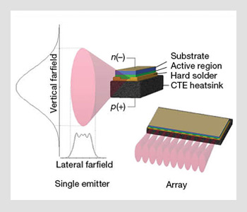 Edge-emitting single-emitter bonded junction side (p) down onto a CTE-matched heat sink that shows anisotropic beam divergence and extension to array geometry.
The downside of these material systems, however, is that they impose design constraints, which in term limit the deployable power and beam-engineering freedom.
Several new techniques have arisen over the past decade to stabilize the aluminum-containing facet at much higher facet loads. These include ion beam oxide removal, surface passivation, quantum well intermixing and cleaving in high vacuums.
These advances enabled the epitaxial and geometrical design freedom of the AlGaAs laser diodes to be exploited such that large spot sizes at the facet could be implemented without loss of performance while reducing beam divergence. High-power AlGaAs diodes in the 900 nm range can now reach >20 W per emitter with deployable powers of ≥12 W per emitter. This has a large impact on the $/watt figure of merit, which now enables the diode power to be beam-shaped and engineered for direct materials processing applications.
The figure above on the right shows a typical high-power edge-emitting laser diode bonded onto a heat sink that has a coefficient of thermal expansion (CTE) matched to that of GaAs (about 6 ppm). The device is bonded active-side-down to improve thermal dissipation as the heat is generated in a very shallow (< 5 µm) region in the epitaxy’s quantum well and waveguide region located on the positive side (p-side) of the chip. Therefore, the active region lies within a few microns from the heat sink surface. Typically, engineers use hard solders such as AuSn, which improve reliability under the extreme thermal fatigue and high current differentials that are associated with the pulsing necessary for materials processing.
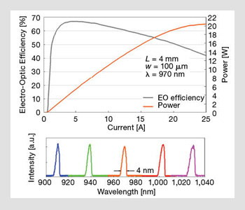 Power and electro-optic efficiency vs. current for a 970-nm broad-area emitter. Lower graph shows spectrums for a range of 900 to 1,050 nm diodes.
For high-power diodes operating in the 800 to 1,100 nm range, a broad area diode has a wide lateral emission region that is typically on the order of 100 mm—which is multimode. The index-guided vertical mode is designed to be single mode with a waveguide thickness of about 1 to 4 µm. Typical high-brightness diodes used for fiber coupling have cavity lengths between 4 and 6 mm; the corresponding number of longitudinal modes is therefore on the order of 100 to 200, where each longitudinal mode has approximately 20 to 30 significant lateral modes.
For each emitter, there are a few thousand modes, each oscillating with a slightly different wavelength. The modes are separated by subangstroms and superimposed to yield a total spectrum of 90 percent power content width of 4 to 5 nm centered in the peak in the gain profile.
The typical wavelength range of state-of-the-art high-brightness diodes is in the 900 to 1,100 nm region. Scientists focus on this wavelength range in part because it represents the pump wavelengths for ytterbium and erbium, but also because reliability increases with wavelength and decreasing photon energy. The top part of the figure on the right shows the power- and electro-optic efficiency from a 4-mm cavity length broad area (wLat= 100 µm) emitter at 970 nm.
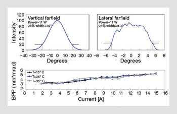 Measured vertical and lateral beam divergences for edge-emitting AlGaAs laser diode in the 900 nm range. The lower graph shows the measured BPP up to a current of 15 A for heat sink temperature excursions of ±10 °C from 25 °C and junction temperatures ranging from 20 to 80 °C.
Typical broad-area emitters reach a maximum power greater than 20 W, with deployable powers in the range of 10–12 W per emitter. Throughout the 900 nm range, the diode performance is nearly uniform with the AlGaAs material system. Wavelength multiplexing allows for beam combining and power scaling up to the kilowatt level while maintaining a low beam parameter product and increasing brightness.
High-brightness diodes can be fabricated as single emitters or arrays, where one chip contains multiple emitters. The advantage of array technology lies in power scaling. Researchers have also developed fiber-coupling approaches—ranging from combining pure single emitters to combining elements from an array with up to 50 emitters on one chip; the benefits of each approach depend on application and brightness needs.
Key features of high-brightness diodes for material processing include not only increased power, lower divergence, and narrow spectrums, but also the stability of these parameters over wide temperature ranges. Processes dictate that diodes be switched on and allowed full thermal loading before being switched off, resulting in junction temperatures varying by 40 to 50 °C during each pulse. Resistance to thermal fatigue requires high adhesion of metallization, dielectric and solder layers, as well as expansion-matching of all materials experiencing the thermal load.
The lateral index profile that supports the multiple lateral modes is created primarily by carrier density variations (injected current and diffusion), but is also influenced by temperature-, strain- and emitter-width-defining processes such as ridge etching, ion implantation and epitaxial regrowth processes. Minimizing and stabilizing the lateral divergence governs the brightness level of the diode and the overall brightness of the multiplexed beam-combined system.
Thus, careful control of these parameters is necessary in order to maintain beam quality over wide current and temperature ranges. Since the vertical beam divergence is diffraction-limited and the waveguide is very narrow (~2 mm), the beam parameter product (BPP) for a broad-area emitter is dominated by the lateral emission. It is given by:
BPPLat = (wLat/2) (θLat/2) ,
where w and θ are the emission width and full divergence angle for the lateral axis.
The top graphs in the figure above show the measured vertical and lateral divergence profiles of a high-brightness edge-emitting laser diode operating in the 900 nm range and operating at 11 W. The lower graph shows the variation of the lateral BPP over current with heat-sink temperature excursions of ±10 °C from 25 °C and junction temperatures ranging from 20 to 80 °C. The brightness (B) of a broad area emitter is given by:
B = P/(π2 BPP2),
where P is the emitter power. The maximum brightness for a broad-area edge-emitting laser is about 120 W/cm2sr and the deployable brightness per emitter is roughly 70 W/cm2sr.
Scaling to kilowatts
High-power, high-brightness diode laser systems are comprised of individual diode lasers. In their most basic units, these lasers are packaged as single emitters or as an array of broad-area emitters. Broad-area emitters can deliver a high level of brightness of up to 70 MW/cm2sr with deployable output powers of more than 12 W per emitter. Compared to single emitters, multi-emitter bars with 20-80 broad area emitters strive for output powers of greater than 200 W.
However, their symmetrized level of brightness merely reaches 10 MW/cm2sr. In order to enable applications such as deep-penetration welding, diode laser systems must enter the kilowatt arena with a level of brightness in the range of 40MW/cm2sr. To achieve this, the individual emitters must be multiplexed using the three common beam-combining techniques: spatial-, polarization- and wavelength-multiplexing.
In the case of spatial multiplexing, individual emitter beams are stacked; thus, power scaling at a constant level of brightness is feasible. By contrast, polarization- and wavelength-multiplexing allow for linear scaling of the brightness by increasing the power at constant beam parameter product. Every commercially available high-power, high-brightness diode laser makes use of these key features: high-power broad-area emitters and multiplexing techniques.
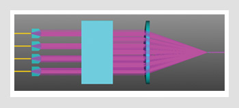 Fiber coupling of diode lasers by spatial multiplexing.
So why has it taken more than a decade for high-power diode lasers to enter the market of high-brightness direct applications? The main reason is that it was not possible to reach the 200 W level of deployable power per bar until advanced broad-area single emitters and hard-solder mounting techniques came along. Another reason is the extremely tight tolerances that result from a highly astigmatic emission profile of the laser diode with an aspect ratio slow/fast axis greater than 60 and strongly differing beam qualities. Due to a fast-axis emission height of approximately 1.5 µm, a well-collimated beam features a rest divergence angle of less than 2 mrad in this direction.
For a single beam, that cannot be regarded as a problem. However, when one is considering spatial multiplexing, he or she must pay careful attention to the multitude of individual beams. Each of them features mm-dimensions and a rest divergence of less than 2 mrad. Thus, every single component in a diode laser system used for beam shaping must feature angular tolerances, which must be measured in respect to the rest divergence angle of the collimated fast axis.
However, current developments to enlarge the fast-axis emission height promise to loosen the critical angular tolerances. The figure above on the right demonstrates spatial multiplexing for fiber-coupling applications. Another important aspect is the so-called “fill factor” of the stacked beams. The vertical fill factor is the ratio of the vertically collimated beam diameter divided by the pitch of the individual beams; obtaining a value near 1 is crucial to establishing a high-brightness diode systems. When one multiplexes a series of single emitters, or the emitters of an array, the system complexity can grow rapidly with the number of emitters deployed. The advantages of both approaches depend on the specific applications for which they are being used.
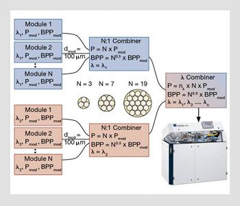 Combining laser modules into a laser unit and laser units into a laser system.
In principle, both single emitters and bars can be the basis for direct diode laser systems. Whereas the single emitter’s benefit is the highest degree of brightness and flexibility, its major drawback is the system complexity, which rapidly grows with the number of single emitters deployed. On the other hand, bar-based systems offer optimum integration by taking advantage of the monolithic bar or stacking of bars; however, they produce a reduced level of brightness, which can be partially alleviated by using intelligent beam-shaping optics.
One approach for combining the advantages of single-emitter brightness and reduced system complexity is to use low fill-factor bars. These only consist of 5 to 10 emitters that perform similarly to single emitters but can still be optically handled as a bar that reduces the number of optical components and manufacturing effort to build a high-power, high-brilliance system.
Laser module
Spatial multiplexing is needed to realize high-brilliance direct-diode lasers. One possible approach is TRUMPF’s TruDiode module. In it, a low fill-factor bar, which incorporates several broad area emitters with a width of approximately 100 µm, is used to generate laser radiation. The beams are collimated in a fast and slow axis. Then they are rearranged and coupled into a 100 µm fiber. The diode module used in TruDiode lasers delivers a laser output of 100 W from a fiber with a diameter of only 100 µm and a numerical aperture of about 0.12. The diode laser bar is mounted to an expansion-matched submount and passively cooled resulting in a long lifetime.
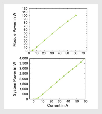 TruDiode system performance. (Top) TruDiode module; 100 W out of 100 µm fiber. (Bottom) TruDiode 3006 high-brilliance multi-kW system at 25 °C water temperature.
Flexible and modular systems
The TruDiode module is the fundamental building block for TRUMPF’s kilowatt-level high-brilliance direct-diode lasers. To scale the power in a first step, one can use spatial combination of module fibers. An especially favorable number of fibers are 3, 7 or 19. A laser unit consisting of several modules and a fiber combiner results in up to 2 kW from a single output fiber with a diameter of 550 µm.
To achieve even higher output powers and brilliance levels, engineers can employ the technique of wavelength combination. After the first fiber combination, a wavelength is transmitted through a dichroic mirror in free space, and the other one is reflected by it, resulting in a beam of twice the power but with exactly the same beam quality as the individual starting beams. This means that the beam diameter and divergence are maintained. In the same way, further wavelengths can be added to increase brightness.
This free space combination also offers the possibility for beam-management through several exits and online power control. Furthermore, the working fiber diameter and NA can be modified. In the case of 19:1 units, a 600-µm working fiber can be used and the NA is reduced to 0.11.
The high brilliance and power make real industrial deep-penetration welding possible with a direct-diode laser, achieving the same, or even better, results compared to lamp-pumped solid-state lasers.
Applications and future outlook
Until now, the most important laser concept for deep-penetration welding has been the lamp-pumped solid-state laser. The typical power range was 1 to 4 kW out of a 600-µm fiber at an NA of 0.1. Through our welding experiments, we have found that deep penetration welding is also possible with a 3-kW high-brilliance direct-diode laser. The achieved penetration is comparable to a standard 3.3-kW lamp-pumped solid-state laser, an HL 3306 D. The surface quality of the welds is very high.
Deep-penetration welding using direct-diode lasers has become a reality. This can be considered as a first step into the high-power laser market, where laser cutting is dominant. The beam quality needed to achieve laser cutting of 5 mm*mrad out of a 100 µm of fiber in the multi-kW-range is a challenge; it would result in an intensity that is 36 times higher compared to a current 600 µm coupled high-brilliance system. Still, it will be possible in the future.
High-power semiconductor lasers, single emitters and bars are developing fast. The achievable powers per device are rising, the efficiency is increasing, and the facet damage threshold is continuously improving. The beam quality in slow axis is also better controlled.
One advantage of the diode laser has not yet been fully exploited. In principle, over a wide wavelength range, any desired wavelength can be custom-made and tightly stabilized. Therefore, dense wavelength multiplexing and very high brilliance levels are achievable. In the century of the diode laser, the possibilities are vast and inspiring.
Stephan Strohmaier, Christoph Tillkorn and Peter Olschowsky are with TRUMPF Laser GmbH & Co. in Schramberg, Germany. John Hostetler is with TRUMPF Photonics Inc. in Cranbury, N.J., U.S.A.
References and Resources
>> J. Bliedtner et al. "Advances in Diode Lasers Increase Weld Penetration," Welding Journal 6, 47 (2001).
>> H. Schlueter et al. "Dense Spatial Multiplexing Enables High Brightness Multi-kW Diode Laser Systems," Proc. SPIE 6104, 61040M-1 (2006).
>> A. Pietrzak et al. "High-power laser diodes emitting light above 1100 nm with a small vertical divergence angle of 13°," Opt. Lett. 33(19), 2188 (2008).
>> S. Strohmaier et al. "TruDiode: Highest efficiency and brilliance for keyhole welding," ICALEO 703 (2009).
>> P. Crump et al. "20W continuous wave reliable operation of 980 nm broad-area single emitter diode lasers with an aperture of 96 mm," Proc. SPIE 7198, 719814 (2009).
>> S.D. Roh et al. "Progress in high-brightness diode laser development based on tailored diode laser bars," Proc. SPIE 7583, 758310-1 (2010).
>> S. Strohmaier et al. "Dramatic advances in direct diode lasers," Proc. SPIE 7583, 75830B-1 (2010).
>> T. Hausken. "Resetting the Laser Market," Laser Technik Journal 7(3), 9-11 (2010).
