
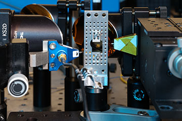
Photonic and terahertz circuits integrated and tested on a single chip. The generated terahertz radiation is collected by the gold mirror in the back to be used for spectroscopy (or sensing) of different materials. [Image: 2025 EPFL/Alain Herzog CC BY SA 4.0]
Terahertz technologies, with operating frequencies between 0.1–10 THz, have important applications in high-speed communications, nondestructive imaging and sensitive spectroscopy. However, current systems typically rely on frequency conversion in bulky and impractical crystals.
Now, researchers based in Switzerland and the United States have developed a hybrid photonic-terahertz chip made of lithium niobate that supports terahertz generation and detection (Nat. Commun., doi: 10.1038/s41467-025-62267-y). The platform—no larger than a coin—paves the way for compact and power-efficient terahertz devices for the next generation of sensing and ranging systems.
Novel hybrid architecture
Lithium niobate is a particularly attractive photonic material due to its ability to generate and manipulate electromagnetic waves across a broad spectrum, from microwave to ultraviolet frequencies. In recent years, the commercial availability of thin-film lithium niobate has enabled the realization of lithium niobate–based photonic integrated circuits on a wafer scale.
“The tremendous progress in lithium niobate technology has prompted us to ask ourselves if this may also become an enabling technology for terahertz applications, by providing a miniaturized alternative to established terahertz systems,” said study author Cristina Benea-Chelmus, École Polytechnique Fédérale de Lausanne (EPFL), Switzerland.
In 2023, Benea-Chelmus and her colleagues created a chip with an integrated photonic circuit made of lithium niobate that, when connected to a laser beam, provided versatile control over the characteristics of a generated terahertz waveform. As a way of building on these efforts, they have developed a novel hybrid architecture consisting of photonic circuits that integrate terahertz transmission lines on thin-film lithium niobate.
More than five octaves
The main component of the chip is a photonics-integrated terahertz transmission line, where an optical waveguide runs between the two signal lanes of a coplanar strip line.
The main component of the chip is a photonics-integrated terahertz transmission line, where an optical waveguide runs between the two signal lanes of a coplanar strip line. With such a design, optical signals and terahertz signals can be routed together on the chip and confined to the same region of space.
“What is really unique is that, by choosing the optical waveguides to be from thin-film lithium niobate and the transmission line to have certain dimensions, we can make sure the two signals propagate at the same speed on-chip for terahertz frequencies that cover a spectrum as broad as 100 GHz to 3.5 THz,” said study author Yazan Lampert, EPFL. “That is more than five octaves.”
By adding antennas, they can operate the chip in two modes, either as an emitter or detector of broadband terahertz pulses. Next, the researchers hope to further miniaturize their system by exchanging several bulky external components for smaller versions, such as lasers, amplifiers, delay lines, modulators and photodiodes.
“Achieving this will not only dramatically reduce cost but will also unlock entirely new applications where size and power efficiency are critical,” said Benea-Chelmus. “Transmission lines, emitters, detectors and resonators are the fundamental building blocks of countless systems. Now that these can be implemented on a single chip, they open the door to terahertz applications in classical and quantum sensing, as well as communication and ranging technologies.”
