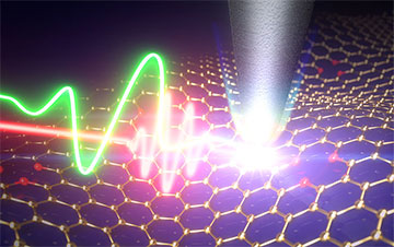
Schematic diagram of the mid-infrared electric-field-driven scanning tunneling microscopy system. [Image: University of Tsukuba]
Scanning tunneling microscopy (STM) leverages the power of quantum tunneling to resolve a 3D atomic-scale map of a metal surface. However, the time resolution of STM has been limited to the sub-millisecond range, which limits the technique’s ability to investigate the ultrafast dynamics of materials.
Now, researchers from the University of Tsukuba, Japan, have reportedly developed an STM system that employs a laser-based pump–probe method to improve the time resolution from picoseconds to tens of femtoseconds (ACS Photonics, doi: 10.1021/acsphotonics.2c00995). This new microscope can visualize physical phenomena that take place at extremely short timescales, such as the rearrangement of atoms during a phase transition or the rapid excitation of electrons.
A pump–probe approach
Optical pump–probe measurements are used to obtain information on ultrafast phenomena. A pump-laser pulse first excites the sample, then after a time delay, a probe-laser pulse hits the sample and its transmittance or reflectance is measured. With this method, the time resolution of the measurement is limited only by the laser pulse duration.
The researchers combine this approach with an electric-field-driven STM, which uses a carrier-envelope-phase-controlled light source to produce a near field to apply an instantaneous electric field between the STM tip and the sample. They aimed to capture ultrafast dynamics in non-equilibrium states, which have applications for both basic and applied material sciences. For example, the new microscope may aid in the design of new solar cells or nanoscale electronic devices.
“In condensed matter, dynamics are often not spatially uniform, but rather are strongly affected by local structures such as atomic-level defects, which can change over very short timescales,” said senior author Hidemi Shigekawa in a press release accompanying the research.
In the team’s setup, a chirped-pulse amplifier with a near-infrared (NIR) wavelength range and pulse width of 8.1 fs is split, with one of the beams being converted to the mid-infrared (MIR). The NIR beam is passed through an optical delay stage and combined with the MIR beam in a coaxial arrangement for pump–probe measurement. They are focused onto the STM tip apex in an ultrahigh-vacuum chamber that houses the sample.
Observing ultrafast dynamics
To verify the technique, the researchers performed time-resolved STM measurements with NIR pulsed light as an excitation and MIR light as a probe. They used a sample of molybdenum telluride, a transition-metal dichalcogenide, which has important non-equilibrium dynamics that appear at timescales less than 1 ps.
The MIR electric-field-driven microscope—with an enhanced time resolution higher than 30 fs—successfully visualized the photo-induced ultrafast non-equilibrium dynamics in the sample over the time range of zero to 1 ps. The observations agreed with the change in band structure associated with the carrier dynamics. The STM system also resolved snapshot images with atomic resolution that could follow the effects of the excitation.
“This level of magnification has been achieved before, but our work represents a significant advance in the temporal resolution available for scanning electron microscopes” said lead author Yusuke Arashida in the press release.

