
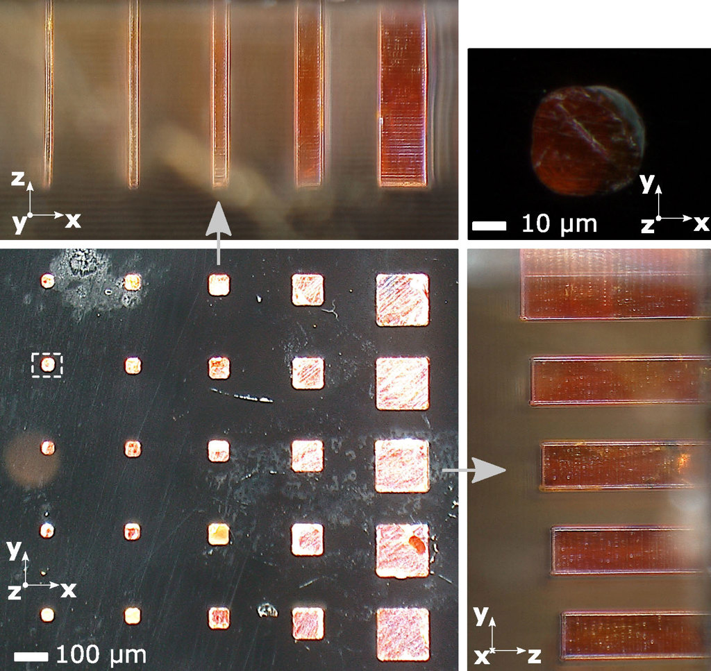
Researchers at a Swiss laboratory used a new fabrication approach to create various structures that combined chalcogenide IR glass with fused silica glass. These included a set of pillars with different dimensions. A white dotted rectangle indicates the smallest silica cavity used in this work. [Image: Y. Bellouard, Ecole Polytechnique Fédérale de Lausanne] [Enlarge image]
For centuries, scientists and artisans have been combining different kinds of glasses to produce results that a single, pure glass cannot achieve. Most of those efforts involve placing two glass types with different properties in contact with each other, creating everything from the crown-flint doublet lens to delicate ornamental glasses.
Now researchers at a Swiss laboratory have developed an infiltration process that pushes chalcogenide glass—a notoriously hard-to-handle substance with a wide transmission window for infrared light—into cavities made of silica glass (Opt. Express, doi: 10.1364/OE.451026). The inventors say the fabricating process could make it easier to create miniature IR optical designs for imaging, sensing and spectroscopy.
Optically strong, mechanically weak
In the last few decades, chalcogenide glasses—those containing sulfur, selenium or tellurium, all grouped with oxygen on the periodic table—have found many applications in optics because of their high transmissibility in the IR region. Their high refractive indices and high nonlinearity also make them favorites for photonic circuits, rewritable optical storage and other devices.
However, glasses in this category are also brittle and age more quickly than other types. Some chalcogenides are especially sensitive to moisture, and a few are toxic to handle, according to Yves Bellouard, a microengineering professor at Ecole Polytechnique Fédérale de Lausanne (EPFL), Switzerland. Freeform manufacturing of mid-IR glass at the micron scale and below has yet to be achieved, he adds.
The infiltration process
The dual-glass fabrication process Bellouard and his colleagues recently developed resembles a similar type of freeform metal micromanufacturing that EPFL devised in 2021. First, the team bombarded a fused silica substrate with a femtosecond ytterbium-fiber laser and then completed the etching stage by soaking the substrate in a sodium-hydroxide bath for several hours.
Once the silica was gone from the laser-irradiated regions of the substrate form, the team put the substrate, topped by a piece of commercially available arsenic trisulfide glass, into a vacuum chamber and slowly heated the interior to 600 °C while reducing air pressure.
While the glasses were still hot, the researchers introduced argon into the chamber until the interior pressure reached 10 MPa. The pressure forced the molten chalcogenide into the cavities inside the silica substrate.
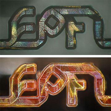
Caption: The researchers fabricated the EPFL logo to show how that the method can be used to make complex 3D shapes. The top image shows dark-field illumination, and the bottom shows bright-field illumination. [Image: Y. Bellouard, Ecole Polytechnique Fédérale de Lausanne]
The EPFL team finished the experiments by testing the fused glasses for spectral transmission and thermal stress and using one of the chalcogenide pillars as a mid-IR waveguide.
Future plans
Bellouard says one of the technical challenges in this research was “related to the specific glass composition used in this proof-of-concept, as one must be careful to avoid any contamination when infiltrating with a fluid that contains arsenic.” Fortunately, the experiment does not require glass containing arsenic; the team just happened to have some of that chalcogenide on hand.
The team wants to expand the applicability of the process to a broad set of interesting glass compositions and size scales, according to Bellouard.
“In terms of applications, we foresee numerous useful uses, notably in portable instruments for gas sensing or mid-IR spectroscopy, and indeed, consumer products where small-scale IR optics are needed, such as high-end smartphones with a capacity for thermal imagery,” he adds.
