

 Engineers working in a microchip lab. [E. Buanoi / Getty Images]
The future of photonics has never looked brighter. Yet that enviable situation is forcing the photonics industry to confront a long-standing quandary: how to train a multi-skilled workforce that can turn that growth potential into reality.
For example, impelled by the needs of AI data centers, “semiconductor packaging is rapidly moving to near-packaged optics (NPO) and co-packaged optics (CPO),” according to Anuradha Agarwal, a principal research scientist at the Massachusetts Institute of Technology (MIT), USA, and head of the FUTUR-IC alliance at MIT’s Initiative for Knowledge and Innovation in Manufacturing (IKIM). But companies, she says, are still “struggling to find ‘photonics-skilled’ employees” who can design and implement these optical solutions.
That struggle goes beyond AI. Rapid technology innovation is requiring nimble approaches to everything from hands-on training to university curricula. Companies, academic institutions, photonic clusters and governments are trying to close the workforce gap.
Pushed into overdrive
Much of today’s interest in photonic solutions traces to AI data centers’ hunger for power and bandwidth, and the need to make those architectures more energy- and cost-efficient. That, Agarwal suggests, has pushed into overdrive the transition from traditional pluggable transceivers to integrated NPO and CPO based on manufacturing-friendly silicon photonics.
 While co-packaged optics for data centers (left) dominate the conversation right now, demand for a skilled photonics workforce is also coming from other application areas, including defense, biosensing, quantum and autonomous vehicles and drones (right). [Getty Images; rawpixel]
“Everyone has heard about these terrifying estimates on just how much power these data centers are going to consume” as industry scales, says Sajan Saini, education director at MIT’s IKIM. Yet some experts, he adds, estimate that “CPO—bringing [light] right up to the chip—can reduce your power consumption 30%, or maybe even up to 50%, for such centers.”
As a result, integrated-photonics solutions are increasingly embraced not only by niche companies marketing custom “optical engines,” but also by giant chipmakers such as Nvidia and Global Foundries. The European Commission’s June 2026 proposal for a “Chips Act 2.0” cited photonic integrated circuits (PICs) and silicon photonics as key strategic technologies.
Beyond AI datacom, Saini sees other end-system drivers accelerating photonic technology. These include ultrafast 5G and 6G wireless, which demands optical solutions to support high carrier frequencies; optical sensing, including lab-on-a-chip medical diagnostics; and 3D imaging and lidar for autonomous vehicles—“not just cars, but drones.” Another area is quantum computing, where platforms could “mix and match” multiple technologies. “It ain’t going to be all photonics,” he admits. “But photonics will definitely play a part.”
Areas such as defense should also continue contributing to growth. For example, former Optica President Stephen Fantone, founder and chair emeritus of Wakefield, MA (USA)-based Optikos Corp., cites the planned “Golden Dome” missile defense system, which could cost some US$1.2 trillion over the next 20 years. To him, this echoes the centrality of optics and photonics in technology advances in other areas such as quantum, AI datacom and medical diagnostics. “When people ask me about the future for Optikos and the things we do,” says Fantone, “I have a one-word answer: ‘More’.”
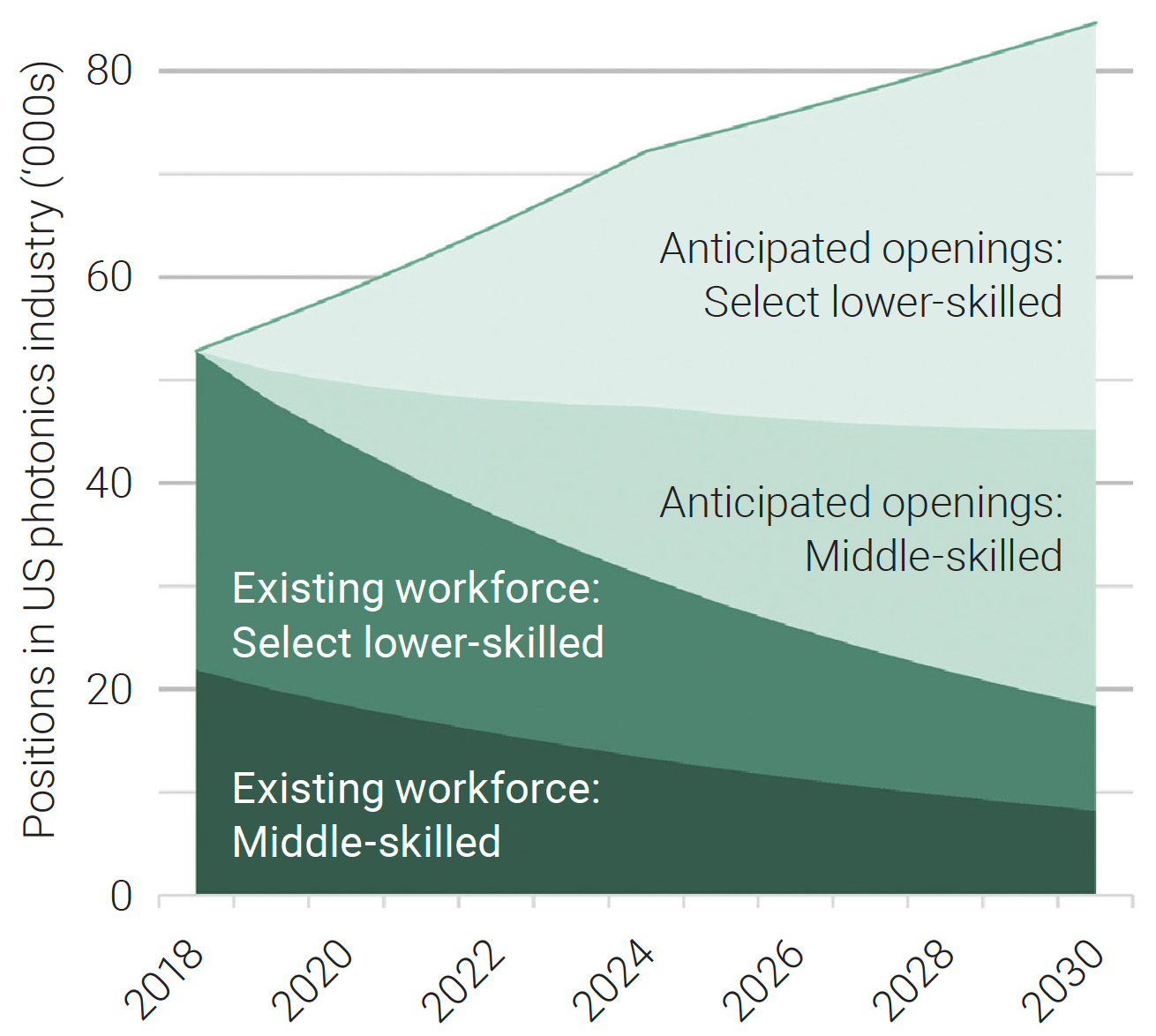 [Enlarge image]A 2023 study in Applied Optics projected that the number of required positions for lower- and middle-skilled technical workers in photonics by 2030 would far outstrip the available workforce. [E.A. Moore et al. Appl. Opt. 62, H9 (2023)]
Feeding an ever-greater appetite for photonics-enabled tech requires a qualified photonics workforce. And right now, experts believe the workforce may not be up to the demand.
Toward “fast reskilling”
Feeding the appetite for photonics-enabled tech requires a qualified photonics workforce. And right now, experts believe the workforce may not be up to the demand. In the United States, the keenest need is for optical and photonic technicians and other “middle-skilled” workers trained below university level. A handful of community colleges offer programs to train and certify photonic technicians. But a November 2023 study estimated that at current graduation rates, another 100 such programs would be required to meet the expected demand for 42,000 new “technical middle-skilled workers” in photonics by 2030. What’s more, these programs will have to offer training “across the supply chain,” in testing, troubleshooting and process design, as well as in critical thinking to foster a sufficiently nimble workforce.
The speed of technological evolution creates training issues up the skills ladder as well. Saini observes that rapid changes in technology, standards and practices mean that “there’s a need to keep overhauling a ‘fast-reskilling’ curriculum” every two years or so. “That’s the challenge.”
It’s a challenge that also applies to developing university engineering curricula and continuing education for experienced engineers. Saini cites the rapid development of CPO, in which THz-scale optical signals must be impedance-matched to GHz-scale RF electrical signals. “If you’re a 45-year-old engineer doing fiber optics, you suddenly have to become really, really literate in stuff you maybe last thought about in an undergraduate electrical-engineering course.”
The current environment also can create skills gaps in areas not so directly tied to physics. Heidi Ottevaere, program director of the Vrije Universiteit Brussel (VUB), Belgium, master’s program in photonics (jointly run with Ghent University), is the coordinator of an EU-funded photonics education network called Phortify. A skills-gap analysis and survey of industry conducted early in the project, she notes, revealed that companies are generally “very happy with the technical background young people have after leaving university.”
Instead, companies saw deficiencies in “the integration of data and digital skills,” as well as in some “transferable” skills such as “entrepreneurship, setting up a business and intellectual property management.” And the survey results stressed a need to “make sure that … students are trained to use AI in a working environment,” she says. “Because they will have to use AI.”
A moving target
How are training efforts coping with these rapidly shifting needs? For MIT’s IKIM, the answer has been to build reskilling options serving workers at various educational levels. IKIM’s offerings include a summer academy on skills-building in integrated photonics for already-hired company employees; a lab-based, hands-on “bootcamp” aimed at community college students considering a photonic-technician track; and programs to fashion university-level curricula in photonics.
The IKIM team continually tracks and refines these programs via the Integrated Photonics System Roadmap–International (IPSR–I), developed in partnership with Netherlands-based PhotonDelta and updated every couple of years. That’s about the right interval, according to IKIM’s Saini, to stay on top of industry changes. “Every one or two years, we understand a bit better the details,” he says. “And that hints at what new things we should add to the curriculum.”
One such “new thing” is what Saini calls “dual skilling”—training that emphasizes the trade-offs between the traditional engineering goal of design for performance, and the need to design for efficient resource use. Coming to grips with those trade-offs, he argues, is crucial amid the continuing build-out of resource-hungry data centers.
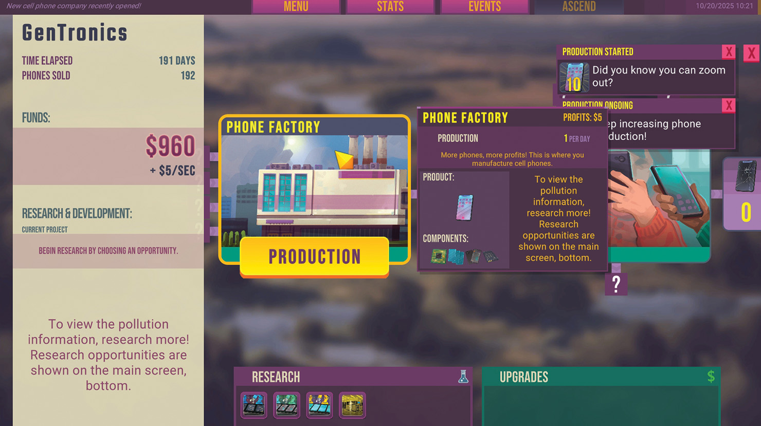 [Enlarge image]GenTronics, an online game developed by MIT’s Initiative for Knowledge and Innovation in Manufacturing, provides “dual skilling” in engineering for performance and resource efficiency. [IKIM / MIT]
GenTronics, an online educational game developed by Saini’s IKIM team, confronts such trade-offs head-on. The game presents users with a specific scenario—scaling up smartphone manufacture—and forces them to balance performance-based design against supply-chain issues and the use of scarce resources such as electricity, water and critical minerals. The team is now working on a level two for the game, centered around designing a data center that might use CPO or NPO as part of the solution.
Close academia–industry connections usually feature prominently in local, regional and national efforts to train the future photonics workforce.
 [Photonics Industries Australia Ltd.]
PIA: Acting locally
Adelaide, South Australia–based Photonics Industries Australia (PIA) is a relative newcomer among photonics clusters. Piers Lincoln, manager of the Adelaide University Institute for Photonics, Advanced Sensing and Quantum Technologies, says the cluster began in the early 2010s largely as an informal effort to connect local photonics companies that “weren’t really talking to each other.” That effort, which produced industry roadmaps in 2016 and 2022, was formally established as a nonprofit in 2024.
As with other clusters, workforce development has proved a key focus for PIA, especially as the South Australian industry has expanded. Between 2016 and 2022, “the turnover [sales volume] and employment levels doubled, which was pretty impressive, I think,” says Lincoln. “That’s when we saw this absolute need for growth in high-level technical staff.”
To meet that need, Laurence Deziel, who joined the effort in 2022, surveyed some 50 local photonics and quantum companies to “ask them what they really wanted,” Lincoln says. The survey results surprised Lincoln. “The US–Canadian community college model of a three-year training program really seemed like the right answer to me,” he says. “But they all said, Nope, we need something quicker than that.”
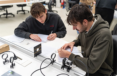
In response, Deziel and the PIA team worked closely with local industry contacts to develop an intensive, 10-day hands-on curriculum to provide the basics—laser safety; fundamental optical tools, techniques and manufacturing; plus three on-site visits with local companies—that would enable them, in Lincoln’s words, “come back and hit the ground running” as productive workers at their companies. “The key, really, is that the whole course has been co-created with industry.”
Launched in February 2026, the 10-day program has thus far mainly served relatively inexperienced new hires at local firms. But Deziel hopes that it can be expanded outside of the cluster’s South Australian current operating area, and offered not just to company employees but to the general public. “A goal of mine is to expand this across the country, helping more people enter careers in photonics,” she says.
GenTronics is “an effective way to get engineers thinking about these trade-offs for the first time,” Saini suggests. “It’s not always a win-win situation.”
The industry–academia nexus
IKIM is also building photonics programs in more-traditional university formats. The team has worked with a local Massachusetts institution, Bridgewater State University, to create what it believes is the first degree-granting undergraduate program in optical and photonic engineering in the New England region of the United States.
Elsewhere, in collaboration with the Abbe School of Photonics in Jena, Germany, the Singapore University of Technology and Design (SUTD) has just launched a one-year, three-term master’s program in optics and photonics technology and design. The program is specifically structured to combine science, computational design, AI integration and hands-on fabrication to prepare students for “impactful roles in industry and research.” In the Netherlands, a similar Master’sPlus program, from a consortium including PhotonDelta, Optics Netherlands and three leading research universities, is likewise dished out with liberal helpings of company visits, industry internships and projects, and other outreach. The student emerges with “an industry-endorsed statement” documenting participation in the program.
Close academia–industry connections of this type usually feature prominently in efforts to train the future photonics workforce. Particularly interesting approaches can emerge from photonics clusters—local ecosystems grouped around one or more academic institutions, private optics and photonics companies, and municipal governments to accelerate industry growth. Such clusters have a built-in incentive to build targeted programs in close collaboration with local industry (see “PIA: Acting locally,” right).
Academic–industry connections also underpin regional and national efforts. A case in point is Phortify, the EU-funded project co-founded in September 2025 by VUB’s Ottevaere and Roberta Ramponi, a retired Italian physics professor and a Photonics21 executive board member, along with colleagues throughout Europe.
At present, Phortify includes seven European universities, three research institutions and two corporate partners. It centers on creating elective packages in emerging areas such as PICs, AI, quantum and biophotonics. The packages draw on photonics courses (in-person and virtual) from multiple consortium universities that can be embedded into the master’s program at the student’s home university.
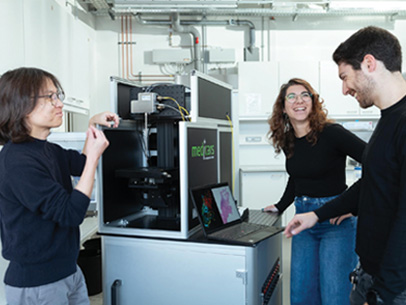 Researchers Hyeonsoo Bae (left), Elena Corbetta and Matteo Calvaresen in the lab at the Leibniz Institute of Photonic Technology in Jena, Germany. The institute is one of 12 academic, research and company partners in the EU-funded Phortify project, which seeks to provide a cross-institution, industry-aware talent development in photonics. [S. Döring / Leibniz-IPHT]
While all this might suggest a top-down, academia-driven effort, Phortify is designed to respond to tangible industry needs. The programs are, according to Phortify, co-designed with industry experts, and include not only the inter-university photonics master’s, but also self-standing modules and “micro-credentialling” options to facilitate “lifelong learning” for researchers and engineers. More important, Ottevaere adds, an explicit goal of Phortify is to create more than 400 collaborations with companies across Europe during the project’s four-year time horizon. The hope is that many of these partnerships—providing internships, master’s-thesis opportunities and other options for hands-on industry experience—will continue long after Phortify’s EU funding officially wraps up in late 2029.
China’s vast canvas
National and regional workforce schemes have one eye on international competitiveness—especially with China, the global leader in photonics market share.
A 2024 study by market research firm Tematys calculated that China held 32% of the worldwide photonics market in 2022, up from 10% in 2005 and compared with 15% each for Europe and the United States. A June 2026 Photonics21 roadmap cited China’s dominance as a key argument for a €2 billion (US$2.3 billion) stand-alone photonics component in the EU’s 2028–34 funding framework.
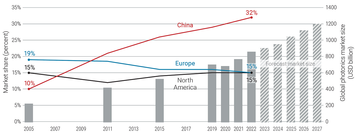 [Enlarge image]China’s rapid growth in photonics market share is a key factor underlying several national and regional workforce development efforts—and also creating new workforce development challenges in China itself. [Photonics21 / Tematys]
Yet rapid growth and technology transformation have given China workforce challenges of its own to meet. Qihuang Gong, an optical scientist and president of Peking University, notes that China is “grappling with a shortage” of mid-tier photonic technicians—which he ascribes to the industry’s “breakneck expansion.” Meanwhile, within the broader photonics workforce, which Gong estimates at 300,000 strong, there’s a “surplus of general application-oriented personnel,” but a “critical shortage” of high-end, cross-trained engineers, process experts and other specialists that can bring expertise spanning optics, microelectronics and precision manufacturing. There’s a geographical dimension as well. The lure of eastern cities and photonic clusters like Beijing, Shanghai, Guangzhou and Shenzhen, Gong says, has made it challenging for industrial clusters in central and western China to attract and retain workers.
These pressures are unsurprising, given the enormous sweep of China’s optics, optoelectronics and photonics undertakings. Gong himself sees three growth areas demanding new skilled workers: integrated photonics and “silicon-based optoelectronics,” spurred by data center expansion; quantum technologies, ranging from computing to encryption to sensors and photodetectors; and new approaches to sensing, lidar and smartphones that will be built on reconfigurable metasurfaces.
More broadly, China’s 15th Five-Year Plan is targeting growth in areas including high-powered lasers and precision and ultrafast lasers for manufacturing; high-speed optical communications and CPO; and “integrated space-terrestrial communication.” The “unifying thread,” in Gong’s view, is that photonics is “stepping out of university and research labs” to become “core foundational infrastructure.”
China’s government has identified optoelectronics and photonics as strategic emerging industries, coordinated across ministries and commissions for “robust, full-industry-chain” support.
China’s government, Gong stresses, has identified optoelectronics and photonics as “strategic emerging industries,” coordinated across multiple ministries and commissions for “robust, full-industry-chain” support.” In parallel, talent cultivation is advanced “in an organized manner” nationwide, an approach that sets China “distinctly apart from many other countries.”
This talent-cultivation effort leverages a network of more than 230 university undergrad programs in optoelectronic industry technology and 100 graduate programs. There are also photonics clusters such as Wuhan’s massive “Optics Valley,” which draws together 42 colleges and universities, 56 research institutes, companies and production facilities, and vocational colleges for minting new photonics technicians. Gong shared with OPN a wide range of other photonics workforce initiatives in China as well, at scales ranging from large new research centers to student awards.
Most of these programs feature tight integration between academic curriculum and industry needs. One interesting example, unveiled in June 2026, is the Shanghai Key Laboratory of Integrated Optical Computing Chips and Systems, built by Shanghai Jiao Tong University and Lightelligence Technology. The center, Gong suggests, could provide a vehicle for cultivating talent in optical computing, integration, benchmarking and other areas.
Overall, however, flexibility will be the key for the photonics workforce of the future in China. “We will no longer judge candidates based merely on a single disciplinary track,” Gong says. “Cultivating versatile cross-field talent will become the core benchmark.”
Boosting photonics in Korea
Across the Yellow Sea, the Republic of Korea knows firsthand the challenges of Chinese competition. In-Ho Bae, a researcher with the Korea Research Institute of Standards and Science and editor-in-chief of K-Light, the magazine of the Optical Society of Korea (OSK), observes that while the display business is “still Korea’s signature strength” in photonics, China dethroned Korea as the number-one display maker in 2021. To compensate, he says, Korea is emphasizing advanced display technologies built on inorganic/micro-LEDs.
Other businesses are driving workforce-training needs. These include optical communications and silicon photonics, spurred by AI data center buildouts, which are “turning silicon photonics engineers from a niche specialty into one of the most sought-after profiles in the semiconductor ecosystem.” Bae also points to sensors, imaging and lidar; quantum technology; defense and aerospace; and laser manufacturing technology, which he describes as “an underappreciated Korean strength.”
One skills gap standing in the way of tackling those markets, in Bae’s opinion, is the need for better capabilities in PICs and CPO design and packaging. That’s partly a policy issue, he notes, as Korea’s current semiconductor strategy is “still built entirely around electrical-signal technology.” Bae also argues that optical engineers need additional fluency in AI and machine-learning techniques as part of their workflows, as well as quantum hardware skills. And technician-level training is, in Bae’s view, “genuinely underbuilt” in Korea, though OSK itself has recently piloted a laser-safety-officer training program for industrial staff.
While government ministries constitute the main funding and policy source for workforce development efforts, the Korea Association for Photonics Industry Development implements several programs on the ministries’ behalf. These include a partnership to train laser-technology graduate students and an “Industrial Innovation Academy” that runs workers from the automotive semiconductor sector through a boot camp for photonics skills. Separately, Korea’s Ministry of Trade, Industry and Resources designates a set of “advanced-industry specialized graduate schools” in priority areas, including semiconductors and displays, that provide training in silicon photonics and display light sources.
In these workforce programs and others, Bae says, the role of Korean government funding is “central, not supplementary.” Much of that funding is organized around 12 national strategic technologies, with semiconductors, displays and batteries in the top tier. In Korea’s draft 2026 budget, the R&D allocation for strategic technologies is ₩8.5 trillion (US$5.8 billion), a jump from ₩2 trillion in the previous year.
None of that spending, though, is earmarked for photonics. While Bae describes Korea as “a genuine manufacturing and integration powerhouse in photonics-enabled products,” he says the country has been “slower than its peers” to treat photonics itself as a strategic area worthy of long-term national commitment. Bae hopes that may change, particularly in light of the rapid maturing of CPO and PICs, which demands laying down a strong workforce pipeline now. “The window to catch up is closing,” he says.
Back to basics
How should undergraduate and graduate students entering photonics improve their odds amid these disruptive forces—AI’s dizzying evolution; global competition; and far-reaching geopolitical factors such as tariffs, warfare and immigration policy?
Andrew Forbes, a professor at the University of the Witwatersrand, South Africa, counsels that what works in the future may not be that different from what worked in the past. “I don’t think it’s changed very much,” Forbes contends. “The core skills that we see people asking for are more or less the same as what they were 10 years ago,” albeit with “a bit more focus on data and AI.”
Instead, thriving in the industry of the future may hinge not solely on specific training programs, academic curricula or government efforts, but on individual creativity and effort. “Obviously, we have to skill [students] correctly,” Forbes says. “But good people will always do great things. And companies will have to try to hire the right people.”
Stewart Wills is a science and technology writer based in Silver Spring, MD, USA.
For references and resources, visit: optica-opn.org/link/workforce.
