
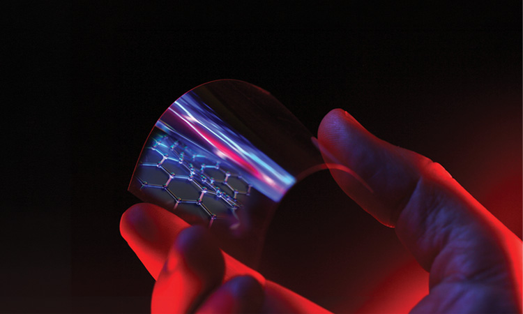
 Lasers are essential for manufacturing flexible OLED and microLED displays. [V. Lombardo / Getty Images]
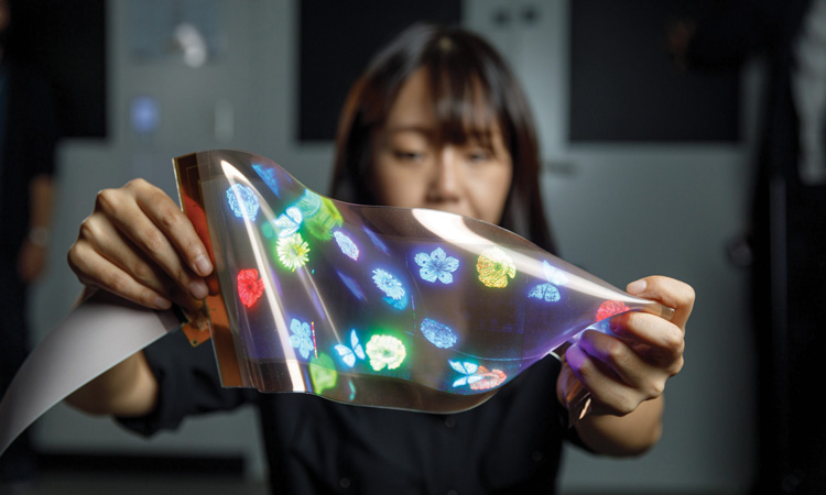
Displays are our main interface to the online world, and recent years have brought rapid progress: ultrathin panels, bendable screens of all sizes, accurate color reproduction and higher resolution and refresh rates.
Behind these developments sits an equally fast-evolving manufacturing toolkit. Display fabs adopt many workflows from semiconductor processing, and lasers have become essential, wear-free tools for heating thin films, cutting and drilling panels, releasing flexible OLED stacks, and transferring or repairing microscopic LEDs. In other words, lasers are not a niche tool in display manufacturing—they are woven into multiple steps that set yield, speed and ultimately cost.
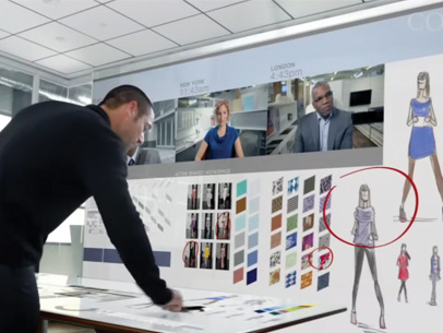 A still from Corning’s 2011 “A Day Made of Glass” video presents a concept for interactive large-format wall and table displays. [Corning Inc.]
From mother glass to pixels: display basics
In 2011, glass manufacturer Corning, Inc., USA, published a video entitled “A Day Made of Glass.” The video, which showed how displays could become enmeshed in our future lives, went viral. Some of the ideas have become reality, while others remain aspirational. At the core of all these technologies is glass, which is also the defining parameter for display “generations.” Most modern panels start on clean mother glass, a solid carrier of the light-emitting layers that are later transferred to the actual display glass.
Mother glass size defines how many displays can be made in one process step and thus, display manufacturing productivity. Thickness also increases with generation to maintain stiffness for ever-larger formats. Although there is no single standardization authority, manufacturers around the globe have largely adopted similar dimensions, as larger mother glass translates into commercial advantage. Mother glass is typically around the millimeter scale in thickness (varying by generation and handling requirements) because it must remain flat and stable through many vacuum and lithography steps.
While mother glass size is mostly invisible to end users (it just defines the price tag), brightness and color gamut are real sales arguments—and they depend on the display technology.
Liquid crystal displays (LCDs) use a white backlight, which is sent through two crossed polarizers with a thin-film transistor (TFT) layer in between. TFTs apply the pixel-by-pixel voltages that control the liquid crystals, which in turn change the polarization so the second polarizer attenuates the light accordingly. A color filter can be added on top of the second polarizer to create full-color images.
Light-emitting diode (LED) displays are active devices: Each pixel generates its own light, so “off” pixels can be much darker than in LCDs and contrast can be higher. Large outdoor video panels commonly use direct-view LEDs, as their pixel pitch (distance from one pixel center to the next) is typically on the order of millimeters.
Organic LEDs (OLEDs) have driven great progress in display quality. They consist of two conductors and a stack of organic materials between them. When voltage passes through, electrons and holes recombine in the organic emissive layer and generate light. But OLEDs’ superior image quality comes with a much higher price, and they are susceptible to burn-in, particularly when static images remain on screen for an extended period.
Active-matrix OLEDs (AMOLEDs) have become standard in high-end smartphones. In an active-matrix design, each pixel is driven by its own TFT and a capacitor. This allows for faster switching, making picture motion smoother. AMOLEDs utilize materials such as polyimide (PI) films. These components are endlessly agile and can fold, bend and even roll.
Quantum dot LEDs (QLEDs) were developed as an alternative to OLEDs. They use nanoscale crystals (quantum dots) that convert blue backlight into highly saturated red and green light, producing vivid color and high brightness.
MicroLEDs are an emerging emissive technology. Each pixel is its own tiny inorganic LED—no backlight needed. With emitters as small as 50 µm and below, microLEDs are positioned as the “next level” after OLEDs. The inorganic material offers longer lifetimes, higher peak brightness, faster switching and improved energy efficiency. But they are harder to make.
Because the different display technologies are at different levels of maturity, the mother glass sizes used in production vary. For example, in 2025, Samsung Display announced its Gen 8.6 OLED plans, starting production in Q3 2026. Samsung also showcased third-generation QLEDs at CES 2024. And Taiwanese manufacturer AUO reported microLED production on a Gen 4.5 line at Display Week 2025.
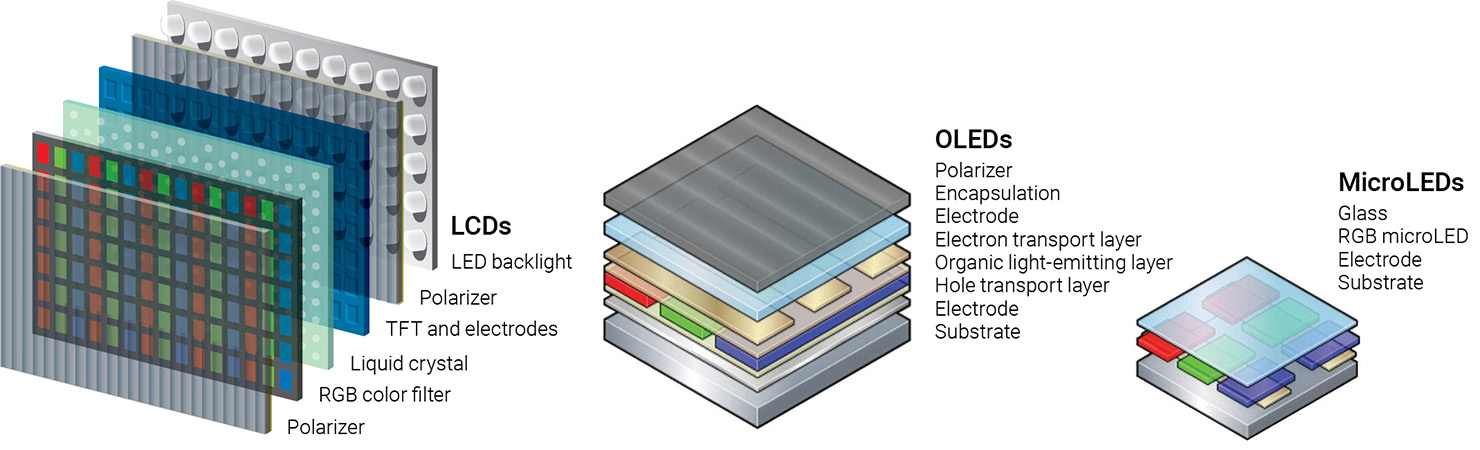 [Enlarge image]Schematic representation of the layered structure of liquid crystal displays (LCDs), organic LEDs (OLEDs) and microLEDs. [Getty Images / Adapted from Delmic]
Silicon annealing with excimer lasers
Modern displays, especially OLEDs, depend on TFTs capable of switching millions of subpixels quickly while maintaining low power consumption, to achieve high refresh rates and long battery life. The performance bottleneck is the semiconductor in the TFT backplane.
In many display lines, a thin layer of amorphous silicon (a-Si) is deposited onto glass by low-pressure or plasma-enhanced chemical vapor deposition. A-Si is easy to deposit at low temperatures, but its disordered structure yields low electron mobility, which limits switching speed and efficiency.
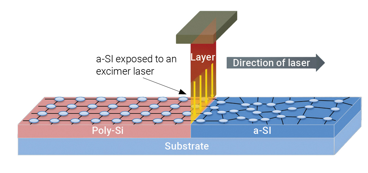 [Enlarge image]Schematic of the excimer laser annealing process. When a-SI is exposed to the laser, it melts and re-solidifies into poly-Si. [Samsung]
This is where excimer laser annealing (ELA) comes in. In a typical OLED panel, the backplane is built from thin layers of a-Si deposited on glass. But the electron mobility there would be insufficient for the requirements of OLED pixels. The a-Si layer must be transformed into low-temperature polysilicon (LTPS), a structure of small crystallites with more than a hundred times better electron mobility.
Conventional furnace annealing cannot achieve this without destroying the substrate, as glass cannot tolerate the required thermal load. The solution is the intense, localized UV radiation (most commonly at 308 nm, which is well absorbed in a-Si) produced by excimer lasers. Because the absorption depth is only tens of nanometers, a nanosecond pulse can melt and recrystallize the silicon surface while keeping the glass substrate relatively cold.
Excimer laser annealing is a masterpiece of innovative technology. The excimer’s rectangular beam is replicated, homogenized and shaped into thin lines by special micro-optics.
The optical system used for ELA is a masterpiece of innovative technology. The excimer’s rectangular beam is replicated, homogenized and shaped into thin lines by special micro-optics. Those segments are added together to form a line that reaches across the width of the mother glass (up to 1.5 m) while maintaining a thickness of 300 to 400 µm and an extremely homogeneous intensity profile.
After annealing, the transistor structure is defined with conventional lithographic methods through a sequence of coating, lithographic illumination, etching and metal deposition. The result is an LTPS TFTs backplane capable of higher pixel density, faster refresh and lower power—key enablers for today’s displays.
These advances underpin high dots-per-inch (DPI) smartphone displays, fast refresh rates for virtual reality and gaming, low-power wearables and high-brightness AMOLED televisions.
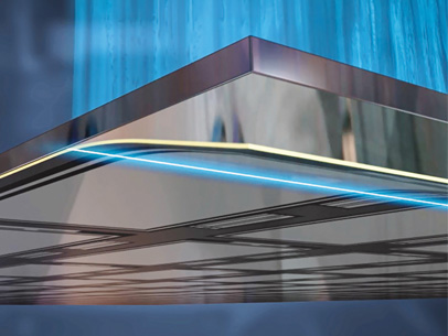 Illustration of the excimer laser LLO process. [Coherent Corp.]
Making flexible OLEDs possible
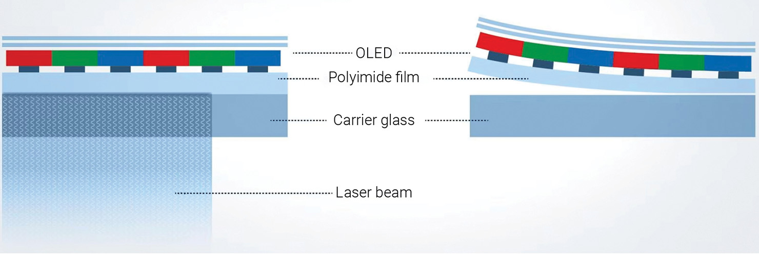
OLEDs are not just brighter and higher contrast than many LCD-based displays, they also enable flexible and foldable displays. The key procedure is laser lift-off (LLO), a laser-based release process that allows manufacturers to build the stack on rigid glass and then transfer it to a bendable substrate through a clean separation process that does not harm the volatile and flexible OLED stack.
In LLO, OLED production starts with a large, ultra-clean mother glass. For flexible OLEDs, a PI layer is first coated onto that glass, followed by fabrication of the TFT layer. Organic layers are then deposited to form the emissive pixels, typically patterned into red, green and blue subpixels using a fine metal mask. Electrode layers are added, and the entire assembly is sealed immediately to protect it from moisture and oxygen, which cause degradation. The detailed sequence of layers is actually more complex than this simplified overview suggests, and some details are proprietary to the manufacturer.
Once the display is completed, the whole system is flipped, and LLO separates the OLED stack from the mother glass. UV light passes through the glass and is strongly absorbed into the PI layer, where it induces rapid decomposition. The OLED stack cleanly lifts off without mechanical or thermal stress.
Excimer lasers used for LLO in display manufacturing (flexible OLED and microLED) are primarily XeCl (308 nm) and KrF (248 nm) lasers, which combine high pulse energy, good beam uniformity and strong absorption by PI/adhesive layers. Solid-state UV lasers are available for the same application; at a wavelength of 343 nm, they can deliver high average power (200 W) with circa 20 mJ pulses.
 [Enlarge image]Schematic of the laser lift-off process for flexible displays. [Trumpf]
Several engineering challenges accompany this:
Beam uniformity: A long line beam must deliver consistent fluence to avoid partial release or damage.
Thermal budget: The OLED layers are only micrometers thick and temperature sensitive. UV LLO must raise only the release layer’s local temperature.
Substrate warping: As displays scale (e.g., Gen 6 and beyond), maintaining a constant focal distance becomes nontrivial.
Debris control: Vaporized polymer can redeposit, so extraction and shielding are critical.
The payoff is enormous: All high-precision patterning occurs on rigid glass, and only at the very end is the flexible form factor realized, enabling foldable and rollable OLED displays at scale.
Cutting cells at high speed
Once the OLED stack is complete, the mother glass panels must be separated into individual display “cells” in a process called cell cutting. A later shape-cutting defines the final outline of the display, including features such as rounded corners or camera holes.
Cell cutting can be done with saws, plasma tools or lasers. Among laser options, CO2 lasers dominate because many stack materials absorb strongly at the CO2 wavelength, allowing efficient cutting with minimal tool wear and low cost per watt—important at volumes of millions of units per month. In some cases, pulsed or q-switched CO2 lasers reduce the heat-affected zone (HAZ), although typically at higher system cost.
CO2 lasers are well suited in cases where some thermal input is acceptable. If that is not the case (e.g. for flexible OLED stacks, thin glasses, sensitive encapsulation layers or displays with tight edge-clearance requirements), manufacturers increasingly turn to ultrashort-pulse (USP) lasers.
 Example of laser glass cutting using a USP laser. [Trumpf]
For flexible OLED stacks, thin glasses, sensitive encapsulation layers or displays with tight edge-clearance requirements, manufacturers increasingly turn to ultrashort-pulse lasers.
With USP lasers, shape cutting becomes far less dependent on thermal effects, making edge quality (and not just speed) the key differentiator. With the trend moving toward ever smaller bezels (or even bezel-free designs), edge quality becomes decisive. The aim is to minimize HAZ and avoid delamination, and USPs are an excellent solution. Repetition rate, scan speed, pulse length and pulse energy have to be optimized for the respective process window. Although 355-nm lasers are established in production, 266 nm may offer higher cutting efficiency, as recent research by Oliver Haupt and colleagues at Coherent Corp. shows.
Precision cutting of glass and sapphire
Another critical step is cutting the cover glass. When smartphones moved from flat rectangles to curved formats, cover glass emerged as a new manufacturing bottleneck. Traditional mechanical scribing can induce microcracks that reduce glass strength.
USP lasers were a game changer, enabling curved edges, notches and small camera cover glasses. Their picosecond (ps) and femtosecond (fs) pulses are absorbed by any material, and the shorter the pulses, the smoother the cutting edge—perfect for processing transparent, brittle materials such as glass or sapphire. Historically, USP lasers have challenged engineers, but after decades of improvements they now qualify for industrial production.
The process window differs for ps and fs systems, with fs lasers still offering less average power and a higher price tag. As a result, both ps and fs lasers are currently used in production for shape cutting and hole drilling, and manufacturers favor different technologies based on HAZ requirements and process maturity.
Cutting without ablation
High-intensity USP laser beams use laser filamentation to cut glass and sapphire. The creation of filaments is a nonlinear effect—namely, self-focusing the USP laser beam, which elongates the focus into a long, narrow filament inside the material and decreases beam divergence.
Filamentation can create a line of needle-fine holes or start a process called “stealth dicing,” in which voids appear below the surface, along the filament path. These voids create a vertical plane of modified material beneath the surface. A clean break along this plane follows, induced by thermal stress or minimal mechanical force. The benefits are smooth edges, minimal subsurface damage, high bending strength (even for thin glass) and the capability to create curved shapes.
This technique is vital not just for smartphones but also for wearables, automotive displays, foldable hinge elements and sapphire-based microLED wafers. Typical chemically strengthened cover glasses (for example, alkali aluminosilicate such as Gorilla Glass) have a thickness of about 0.5 mm, while some foldable displays can be as thin as 30 µm.
Because USP lasers operate in pulses, repetition rate is crucial for throughput. Filamentation requires pulse energy above a certain level to achieve the desired modification depending on material and focal diameter. It must not go far beyond the modification threshold to avoid glass melting or cracking.
During filamentation, the beam is focused inside the transparent material. Each pulse (or pulse burst) generates a narrow energy filament through the bulk of the material. Voids form that are smaller than the laser beam diameter. Within the laser beam diameter, the material is modified: It is densified, with seeds for microcracks. Localized heating along the line then drives controlled crack propagation and complete separation, producing a clean edge with few microcracks away from the cut.
For this process, the USP laser beam is scanned across the surface and each pulse (or burst) produces a single filament zone all the way through the glass (typically spaced about 50 µm apart), forming a vertical cleavable plane. This will allow the part to be separated. A CO2 laser can be used to generate very localized heat stress along the filament line.
 [Enlarge image]Laser-based transfer can place individual microLED pixels or larger dies containing multiple emitters. [Coherent Corp.]
Enabling the next display paradigm
MicroLEDs are widely considered the future of premium displays; they combine the brightness and robustness of LEDs with the pixel density and thinness of OLEDs. While LEDs have a pitch in the order of millimeters, state-of-the-art microLEDs target 50 µm, and a 10 µm pitch, which would correspond to 2540 dpi, may be within reach in the coming years. And they can be turned on and off in nanoseconds, which would make them interesting for data exchange between microprocessors.
The manufacturing challenges are immense. A single display requires millions of micro-scale LEDs, each of which must be produced, transferred, positioned and tested—creating multiple opportunities for sophisticated lasers.
A single display requires millions of micro-scale LEDs, each of which must be produced, transferred, positioned and tested—creating multiple opportunities for sophisticated lasers.
Most gallium nitride (GaN) microLEDs are grown epitaxially on sapphire wafers, commonly 150 mm and 200 mm, with larger formats under development. For display assembly, the GaN layer must be moved from the wafer to a display backplane. A proper LLO for these chips is similar in concept to OLED LLO; a UV laser separates the GaN epitaxial layer from the sapphire substrate.
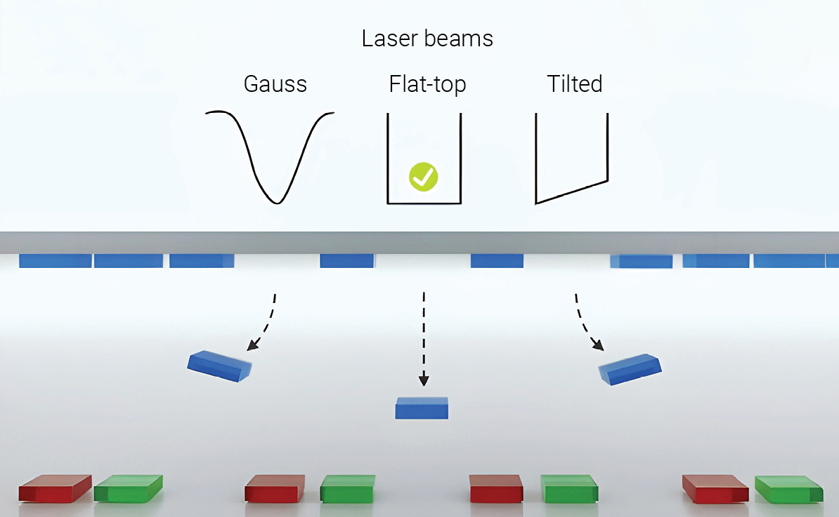
After release, microLEDs must be placed onto a backplane quickly, accurately and at scale. The method of choice is laser-induced forward transfer (LIFT). In LIFT, a single laser pulse can launch thousands of microLEDs from a donor substrate onto the target, dramatically reducing assembly time for small-pitch displays such as AR microdisplays or high-resolution screens.
It may feel counterintuitive that a laser can physically move hardware. In the LIFT procedure, pulses from a UV (excimer) laser shine through the transparent back side of the carrier. The light is absorbed in a release layer, inducing photochemical bond breaking. A highly uniform flat-top beam profile evaporates the layer and propels the pixel onto the final display panel, which is placed at a controlled gap (large enough to prevent collisions). Adhesive on the receiver substrate holds the microLEDs in place. Importantly, the transferred material need not melt, and direct mechanical contact between donor and receiver is avoided.
Several variants of this concept have evolved. First, LIFT can transfer thousands of LEDs in parallel from a circular wafer to a rectangular backplane in a version also called mass transfer. In case of missing or defective pixels, LIFT can also place a new microLED at the right location with micrometer precision, enabling pixel repair and rework.
 LG’s Stretchable microLED display can be extended, folded and twisted without distortion or damage. [LG Display]
From lab to fab
The trends in display manufacturing are obvious: Larger mother glass allows the fabrication of cheaper or bigger panels. Brighter displays with smaller pixels conquer new markets such as extended reality (XR), and flexible displays are revolutionizing automotive entertainment. The vision of ubiquitous screens integrated into windows, walls, tablets, dashboards and other everyday surfaces in the “A Day Made of Glass” video may be an accurate portrayal of what comes next.
Turning that vision into reality depends on a strong ecosystem, in which research results are efficiently transferred into industrial processes. Laser development tracks design trends closely. Shorter wavelengths enable smaller features, ultrashort pulses promise superior edge quality, and higher power and better beam shaping raise throughput. So far, CO2 and excimer lasers have retained their position in fab workflows. Only dramatic technical or cost benefits justify introducing a new laser into production lines.
The development of much of the underlying laser technology is done at a few specialized companies and their partners. Laser manufacturer Coherent, for example, runs a dedicated UV application lab at the Fraunhofer Institute for Laser Technology (ILT) in Aachen, Germany. A team there has the tools and the expertise to refine and validate processes until they are ready for 24/7 deployment.
The continued growth of display markets—from mobile and wearable devices to automotive and XR applications—relies on an ecosystem in which research institutions, engineers and manufacturers jointly advance the maturity of laser-based processes. In this environment, applied photonics becomes a competitive edge: It turns promising concepts into processes capable of sustaining high-volume production. This way, a multibillion-dollar market evolves, bringing more glass-enabled, screen-rich innovations into everyday life.
Andreas Thoss (th@thoss-media.de) is a freelance writer based in Berlin, Germany.
References and Resources
-
Corning Incorporated. “A Day Made of Glass … Made Possible by Corning” (2011), corning.com/emea/de/innovation/a-day-made-of-glass.html.
-
O. Haupt et al. “UV and DUV laser cutting of OLED displays for an enlarged active area,” Proc. SPIE PC13351, Laser-based Micro- and Nanoprocessing XIX, PC133510B (2025).
- F. Werr et al. “Ultra-short-pulse laser filaments for float glass cutting: Influence of laser parameters on micro cracks formation,” Front. Phys. 10: 862419 (2022).
