
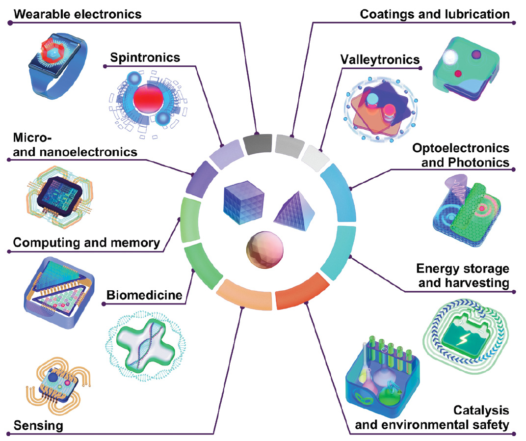
 [Enlarge image]Potential applications of geometrically precise van der Waals nanoparticles.
The vast family of van der Waals (vdW) materials, numbering in the thousands, holds immense promise for revolutionizing optics and photonics.1 Their unique properties, including giant optical anisotropy and record-high refractive indices, offer a path to overcoming the diffraction limit and creating next-generation optical devices. Yet much of this potential remains unrealized. Progress in the field has been constrained by a critical bottleneck: the lack of a universal and scalable method for nanostructuring these materials. Until now, fabrication has relied on bespoke, slow and material-specific protocols that have left the full potential of the vdW library locked away, relegating fabrication to artisanal, one-off processes.
This work shatters that bottleneck with a simple yet powerful method: femtosecond laser ablation and fragmentation in liquid.2 This approach acts as a universal chisel, capable of carving bulk vdW crystals into pristine nanoparticles with exquisite control. Its universality has been demonstrated across an unprecedented library of over 50 different vdW materials, including transition metal dichalcogenides, MXenes and perovskites. More remarkably, the technique produces a diverse array of exotic, highly crystalline nanoshapes determined by each material’s intrinsic properties. The synthesis has forged everything from perfect spheres and fullerene-like polygons (MoSe2) to equilateral nanopyramids (WTe2) and crystalline nanocubes (MAPbBr3).2
For the optics community, these nanoparticles represent a new palette of high-purity, high-refractive-index, ligand-free building blocks for nanophotonics.3 The ability to deterministically create unique morphologies such as pyramids and cubes introduces an entirely new degree of freedom in device design. In nanophotonics, geometry dictates the resonant confinement of light. This method allows designers to select materials not only for their refractive index but for the specific nano-resonator shapes they naturally adopt. This capability enables unprecedented control over Mie and excitonic resonances, which is essential for engineering advanced metasurfaces, high-resolution structural color, resonant nanoantennas and quantum emitters.4,5
This breakthrough delivers more than a new synthetic route; it provides a complete, scalable fabrication platform that bridges the gap between laboratory curiosity and industrial fabrication. With synthesis rates reaching up to 100 mg/h for materials such as gold and demonstrated scalability to grams-per-hour levels, the method is fast and potentially more cost-effective than traditional wet chemistry.2 By providing a true nanophotonic toolkit spanning over 5,000 vdW materials, this work is poised to accelerate innovation across a spectrum of light-based technologies, from on-chip optical computing and high-efficiency photovoltaics to biomedical theranostics and next-generation sensing.2
Researchers
G.I. Tselikov, A.A. Minnekhanov, G.A. Ermolaev, G.V. Tikhonowski, I.S. Kazantsev, D.V. Dyubo, D.I. Tselikov, A.A. Popov, A.B. Mazitov, S. Smirnov, N.D. Orekhov, I. Kruglov, A.V. Syuy, A.V. Arsenin and V.S. Volkov, XPANCEO, United Arab Emirates
D.A. Panova, King’s College London, UK
F. Lipilin, U. Ahsan and Z. Sofer, University of Chemistry and Technology Prague, Czechia
A.V. Kabashin, Aix-Marseille University, France
B.N. Chichkov, Leibniz Universität Hannover, Germany
K.S. Novoselov, National Univ. of Singapore, Singapore
References
1. F.J. Garcia de Abajo et al. ACS Photonics 12, 3961 (2025).
2. G.I. Tselikov et al. ACS Nano 19, 22820 (2025).
3. P.G. Zotev et al. Laser Photonics Rev. 17, 2200957 (2023).
4. V.E. Babicheva et al. Adv. Opt. Photon. 16, 539 (2024).
5. A.V. Prokhorov et al. Nano Lett. 23, 11105 (2023).
