
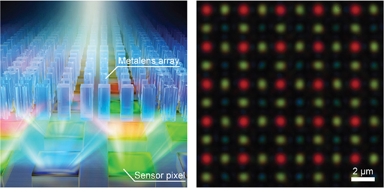
 Left: Schematic of a high-sensitivity image sensor with a color-sorting metalens array. Right: Microscope image of a focal-plane light profile of a color-sorting metalens array under white-light illumination. [Enlarge figure]
Image sensors serve as the eyes of a machine and lie at the core of cutting-edge technologies such as smartphones and autonomous vehicles. These technologies have always spurred high demand for the creation of high-sensitivity image sensors that enable dark-scene and ultrafast imaging. Conventional image sensors employ light-absorptive color filters on every pixel to extract color information. Unfortunately, the light-filtering operation of this architecture, which essentially limits the detectable light amount per pixel, has been a long-standing barrier to sensitivity improvement.
Several approaches have been proposed to remove the filters, but it is still challenging to achieve a filter-free sensor while providing high color-image quality and compatibility with current CMOS sensor technology. Therefore, traditional filter-based sensors still dominate today, despite their inherent sensitivity limitations.
To resolve this contradiction, we recently demonstrated a CMOS-compatible, pixel-scale metasurface-lens (metalens) that collects light while sorting primary colors on high-density pixels. This allows us to replace the absorptive color filters with transparent color sorters in CMOS image sensors, which in turn maximizes the detectable light amount on every pixel and thereby boosts their sensitivity.
Miniature color sorters have been demonstrated by several research groups, including ours, but thus far they have exhibited poor color-sorting efficiency and strong incidence-angle dependence1,2 or have required complex 3D nanostructures,3 far from the fundamental requirements in current CMOS sensor technology and applications. In our recently published work, by leveraging a metasurface platform with rich color dispersion, we created novel pixel-scale metalenses for color sorting while maintaining consistency with state-of-the-art sensor technology.4
Our metalenses simultaneously act as efficient color sorters and lenses, even in the form of CMOS-compatible binary patterns. They are also consistent with the Bayer pixel arrangement, a widely adopted color pixel arrangement in image sensors. In addition, their efficient light focusing makes them highly resistant to oblique light incidence with imaging optics. Thus, these metalenses offer a promising path toward straightforward replacement of filters by sorters in current image sensors.
Using such metalenses, we demonstrated filter-free image sensor architectures with a roughly 2.9-fold enhancement of detected light on high-density pixels; high color-image quality with reduced impact of sensor noise; and compatibility with widespread imaging optics, including smartphone cameras. We believe that these demonstrations will open the way to the development of high-sensitivity color image sensors that exceed current sensitivity limitations without sacrificing image quality, can be implemented in conventional imaging optics, and are consistent with current sensor manufacturing. This work also points to the potential of metasurface optics to drastically boost the performance of consumer optoelectronic devices.
Researchers
Masashi Miyata, Naru Nemoto, Kota Shikama, Fumihide Kobayashi and Toshikazu Hashimoto, NTT Device Technology Laboratories, NTT Corp., Atsugi, Kanagawa, Japan
References
1. S. Nishiwaki et al. Nat. Photon. 7, 240 (2013).
2. M. Miyata et al. ACS Photon. 6, 1442 (2019).
3. P. Camayd-Muñoz et al. Optica 7, 280 (2020).
4. M. Miyata et al. Optica 8, 1596 (2021).
