
Scatterings
Nanotubes Soak Up the Near-Infrared Sun
Researchers at the Massachusetts Institute of Technology (U.S.A.) have devised an all-carbon, near-infrared photovoltaic cell filled with single-walled nanotubes.
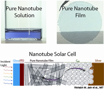 Top: Single-chirality carbon nanotubes in solution (left) and as a film (right). Bottom: Cross-sectional diagram of the near-infrared solar cell.
By exploiting the strong ability of carbon nanotubes to absorb infrared wavelengths, researchers at the Massachusetts Institute of Technology (U.S.A.) want to harvest the portion of the solar spectrum that we can’t see. The team has devised an all-carbon, near-infrared photovoltaic cell filled with single-walled nanotubes (Adv. Mater., doi: 10.1002/adma.201202088).
Silicon photovoltaic devices are great for collecting visible sunlight—but 40 percent of the incoming energy is in the infrared. Other possible technologies for generating electricity from the sun’s near-infrared rays, such as quantum dots or small-molecule organic substances, absorb both infrared and visible rays, says lead author Rishabh Jain, a doctoral candidate in Michael S. Strano’s chemical engineering group at MIT. Not only do the carbon nanotubes selectively absorb near-infrared light, but they are stable in air—an important consideration for building a practical device.
The optical properties of carbon nanotubes are highly specific to the structure of the tubes, Jain says. Isolating the desired tube shapes is one of the more challenging tasks in nanotube studies. The MIT team used a newly developed gel-chromatography method to isolate the tubes of the desired chirality.
Light enters the device through a supporting glass substrate coated with indium tin oxide and passes through a 100-nm-thick film of 0.7-nm-diameter carbon nanotubes, which acts as the p-type junction. A layer of C60 molecules, so-called “buckyballs,” forms the n-type material, and an electrode of thermally deposited silver captures the electrical current.
With open-circuit voltage of 0.33 V, the proof-of-concept device generated 0.81 mA per square centimeter at an overall efficiency of 0.1 percent. Jain and his colleagues want to increase the efficiency of the carbon cell by aligning the nanotubes within the film, instead of depositing them in random orientations. The interfaces between component materials could be optimized to control the cell’s electronic properties better. Jain hopes to get the device up to 20 percent efficiency and combine the cell with a silicon cell to extract more energy from sunlight than traditional silicon photovoltaics alone.
Log in or become a member to view the full text of this article.
This article may be available for purchase via the search at Optica Publishing Group.
Optica Members get the full text of Optics & Photonics News, plus a variety of other member benefits.
