
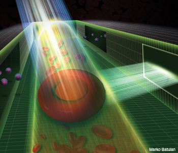
 Optofluidic platforms advance the use of optical technologies in biomedicine.
Microfluidic devices are ubiquitous due to their flexibility and the ease with which they can be fabricated. These thumbnail-sized machines consist of complex structures such as fluid pumps, valves, reservoirs and sorting chambers built around microscopic channels where processes as diverse as optical interrogation and optical sorting take place often simultaneously when combined with optical elements. They can be used to trap and manipulate particles, perform chemical sensing, or map shear stress.
Optofluidic chips, as they are commonly known, have inherent advantages over conventional optical tools that interrelate with fluidic interfaces in more traditional ways. For example, because they are designed and built using equipment and methods borrowed from optical lithography, chips can be easily produced in mass scales at low cost, with short design cycles and miniaturization naturally attained as an added benefit. In addition, the materials that are most commonly used for these devices are inert and robust, making optofluidic systems easy to incorporate into designs that include biochemical assays, single cells and even combinatorial chemistry processes.
Although optofluidics is a relatively new field of research, scientists and engineers around the world have already achieved important landmarks using optofluidic tools: By integrating microfluidic networks of channels with optical components in innovative ways, research groups have found useful ways of making light interact with particles in a controlled environment. To date, entire journals are dedicated to the dissemination of research in this area, and groups within research institutions devote most of their efforts to advancing the field.
Flowing liquids are an inherently good mechanism for transporting microscopic particles. This natural characteristic of liquids is critical for creating chemical reactors and devices for the biochemical analysis of particles, since fluids can serve both as carriers of specimens and active reagents. In addition, variations of the local optical properties can be readily induced by introducing a change in their composition—for example, by introducing mixtures of specific agents with concentrations to modify their refractive index or absorption coefficient.
At the microscopic scale, the boundaries between immiscible fluids constitute smooth surfaces, from which controlled streams of liquids or highly monodisperse droplets can be extracted at controlled rates, creating emulsions that can serve as minute vessels for moving even smaller objects with an unprecedented level of control.
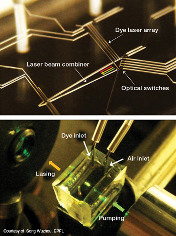 Air-controlled optical elements. (Top) Close-up view of the microfluidic structure of a multi-color dye laser which contains dye laser array, optical switches and beam combiner. (Bottom) Pneumatically tunable optofluidic dye laser chip in operation. The wavelength can be selected by optical switches. The lasing output can be either single wavelength or the combination of beams from the dye laser array.
Lab-on-a-chip
The holy grail of optofluidics is arguably the complete integration of a fully operational device within a chip, often referred to as lab-on-a-chip. Undoubtedly, an entire range of applications would benefit enormously from a portable optofluidic instrument that is embedded completely in a postage-stamp-sized wafer with no material attachments to other external equipment. Researchers engaged in early initiatives in this direction have sought to integrate a coherent light source within the device. Although this would be a natural first step, it is not a straightforward task.
The fabrication of a laser within the planar geometry of an optofluidic chip is a noteworthy advancement in the direction of full integration. Researchers from Harvard University and the Massachusetts Institute of Technology effectively constructed an integrated dye laser on a chip. The source produced a bright spectral line, tunable over the range of emission of the dye. Their ingenious resonator design was based on a waveguide where both the cladding and the core materials were fluid phases susceptible of being reconfigured by flow control. This work represents a major step towards a laser source that is part of the optofluidic device and not an external piece of equipment.
More recently, scientists from the School of Engineering at the Swiss Federal Institute of Technology in Lausanne, Switzerland (EFPL)—one of the most productive groups in the field—have demonstrated a pneumatically tunable dye laser. Sophisticated in design, their laser comprises an air-gap etalon within the chip that serves as the wavelength-tuning mechanism. When pressurized air is introduced in the gap, the wavelength of the laser is selected from a range spanning 14 nm. The group also developed other air-controlled optical elements in conjunction with the laser, including optical switches, in-plane lenses and optical modulators. "Compressed air has been extensively adopted to manipulate the fluids on the chip," says Wuzhou Song, a young researcher at the Optics Laboratory at EFPL. "The air-tuning method turns out to be a very versatile approach to control various optical functions on a microfluidic chip. Aside from being fully compatible with conventional chips in terms of fabrication and control, the air tuning also features fast response and low cost."
Another challenge in integration is figuring out how to include optical mechanisms for manipulating particles within the devices. Many approaches have been used in search of an optofluidic platform that is capable of immobilizing and allowing time for the comprehensive optical analysis of microscopic particles of interest. The goal is a complicated one due to the effect of Brownian motion, the interactions between particles under study and the wall surfaces of the device, and the high level of control required for the task.
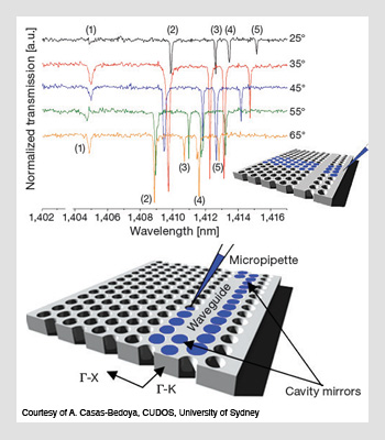 The optofluidic tuning of PhC waveguides. (Top) Normalized transmission spectra as a function of temperature during the probe of an optofluidic PhC cavity 6.8 µm in length. (Bottom) Fluid infiltration of a photonic crystal cavity; a micropipette is used to modify the dispersion engineering of a waveguide. Note the defect waveguide and the PhC mirrors on each end.
Researchers from the University of St Andrews in Scotland tackled this problem by fabricating a network of microfluidic channels using laser material. Using this approach, they successfully guided and trapped microscopic particles within the channels, while at the same time opening the possibility of detecting single particles with optical means. Lasers built in the same planar device were used to create dual-beam traps and an optical guiding beam. This method allowed for optical manipulation without requiring an external laser or the high-numerical-aperture optics that are typically used in traditional optical tweezers.
More recently, researchers at the Erickson Lab at Cornell University demonstrated a silicon photonic crystal device that is capable of performing particle trapping based on optical resonances. Used in conjunction with carefully engineered waveguides, their resonator can simultaneously trap and propel particles at the nanometer scale with stiffness that is comparable to or higher than that achieved with state-of-the-art optical traps. The geometry and fabrication techniques used in this device constitute a promising possibility for manipulating single molecules.
Also at Cornell, researchers in the nanophotonics group have gone one step further—by successfully demonstrating optical trapping with evanescent, broadband coherent radiation from a supercontinuum laser. In this elegant combination of controlled fluidic transport and optical manipulation, light is generated outside the device and introduced using a tapered fiber lens.
One particularly ingenious way of holding a particle in place is to monitor its random displacements precisely and then nudge it in the opposite direction quickly enough that the particle will experience a nearly zero force and therefore a minimal displacement. At the Moerner Lab in Stanford University, scientists have actually managed to look at the activity from a single molecule for more than one second, a rather long time compared to the frequency of displacement of the molecule. Using real-time feedback to control the Brownian motion of the individual molecules, the movement of the particles is effectively canceled out by an externally applied electric field, therefore immobilizing individual molecules in solution.
Regulating flow
In order to properly operate an optofluidic device, one must be able to precisely control the channels through which samples and materials flow within the microscopic system. At the scales involved, the viscosity of all the fluids becomes increasingly important as the fluid velocity increases and the dimensions of the channels are reduced, therefore presenting significant resistance to movement along the channels. In addition, most applications include the flow of rather small quantities of liquids, ranging in volume from a few microliters (µl) per second to a few picoliters (pl) per hour.
For these two reasons, it would be desirable to develop optofluidic-based machines that have an on-chip mechanism for accurately regulating the mass flow rate over a large span and with long-term stability. An interdisciplinary research team from the University of Virginia, Auburn University and Pennsylvania State University has recently devised a clever method for solving this problem. In their approach, the team demonstrates how to precisely control the flow with thin, deformable membranes that respond to the frequency of a time-modulated pressure source. These flexible membranes react to pressure changes in much the same way that passive electrical circuit elements respond to AC electric signals; they effectively achieve on-demand selective flow switching.
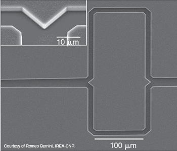
Several materials have been used for building optofluidic platforms. Among the all-time favorites is polydimethylsiloxane, or PDMS for short—an inexpensive polymeric organosilicon with variable viscoelastic properties that allow it to be molded and subsequently cured with heat. Depending on the requirements of the application, however, photosensitive polymeric resins, thermoset plastics, amorphous glasses and even crystalline semiconductors have been used as the bulk substrate in which the features of the devices are built.
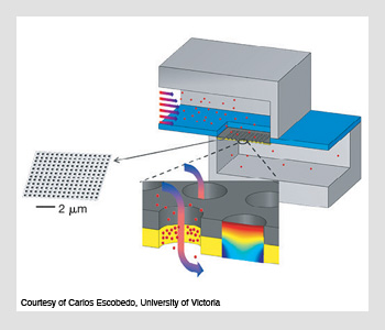 The flow-through nanohole-array-based sensing platform. The nanoholes are milled through gold-on-silicon-nitride membranes using focused ion-beam lithography. Target molecules flow through the nanoholes and bind to the functionalized inner gold surface, which provides a measurement for sensing. An image of the computational simulation results of the concentration profile of target molecules is shown in the cross-sectional nanohole detail.
In addition, in recent research efforts, scientists have combined microfluidics with fabrication processes borrowed from other fields of optics. Australia's CUDOS (the Centre for Ultrahigh-bandwidth Devices for Optical Systems of the University of Sydney) is one of the pioneering optofluidics groups worldwide; there, researchers have engineered the dispersion of waveguides made with photonic crystals (PhC) infiltrated with liquids in their periodic holey structures. PhC microscopic structures are well known for strongly controlling light on the wavelength scale. In addition, due to their periodic air-hole microstructures, they are well-suited to optofluidic tuning and thus natural candidates for housing liquids.
In contrast to traditional lithographic processes, the optofluidic tuning of PhC waveguides is completely reversible and limited only by the properties of available fluids. Their approach provides an efficient and versatile method to modify waveguide dispersion after the fabrication stage. As Alvaro Casas-Bedoya, a young researcher at CUDOS, explains: "In combination with photonic crystals, the features in optofluidic devices are ideal for use in medical diagnostic tests based on the formation of antigen-antibody complexes."
Challenges and applications
However, a pervasive problem in molecular-level biomedical applications is the low concentration of biomarkers in clinical samples and the inefficient transport of these molecules to a functionalized surface, which limits the detection capabilities of existing sensors. In a different application of ordered holes at the nanometric scale, Carlos Escobedo and his colleagues from the University of Victoria in Canada have shown how periodic arrays of holes machined in a metallic film can be used in a flow-through sensing scheme for the early detection of cancer.
 Optofluidic flow cytometer. This device provides statistical information on subpopulations within a sample, such as the relative ratios of various types of white blood cells, by measuring the properties of each individual cell. This platform leverages the precise control of microfluidics while further offering robust, pre-aligned optical elements, all on a low-cost cartridge that is ideal for biohazard containment.
In their research, which they presented at the 2010 Conference on Lasers and Electro-Optics (CLEO), they have quantified the influence of chemical binding rates and the transport of biomarkers to the sensor's surface. The performance of their sensing scheme suggests that the flow-through operation scheme offers at least a 10-fold improvement in sensing time response for typical sensing parameters. The principle of operation is simple, according to Escobedo: "Light passing through arrays of ordered nanoscale holes in metal films exhibit enhanced transmission at specific wavelengths, which appear as peaks in the light transmission spectrum. Any small change in the refractive index of the medium in the vicinity of the array or in the condition of the metallic surface shifts the peaks observed in the transmission spectrum."
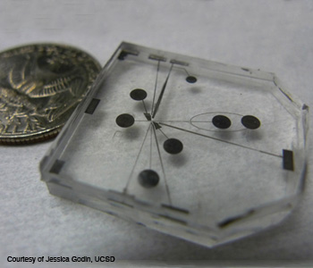
The small footprint of optofluidic devices has inspired researchers to replace current technology with more compact and sometimes more reliable instruments. Such is the case of the flow cytometer developed by researchers at the University of California, San Diego. "Flow cytometry is used to study, diagnose and monitor many health and disease states," says Jessica Godin, a young professional with the research group. "A massively fabricated, lower cost flow cytometer would help move this critical tool from shared core facilities into every lab and clinic, allowing for rapid results and more flexible experimental design."
Inside their cytometer, which is the size of a U.S. quarter, cells are individually transferred past a laser beam while the device detects light scattered from the cells as well as the fluorescent emission from antibody tags. By exploiting the slight angular difference between refraction and total internal reflection, the researchers have successfully created waveguides that preferentially include light originating from the cell and that exclude light coming from short distances. This solves the ever-present problem of low signal-to-noise ratio in fluorescence measurements. In Godin's words, their technique may allow for a truly integrated, low-cost optofluidic flow cytometer cartridge with performance rivaling that of a standard commercial device. The mold-replicated device integrates tapered, solid-core waveguides and optics in a monolithic design that is easy to reproduce.
 Optofluidic MZI fabricated with hollow-core waveguides. The waveguide cladding materials were deposited in layers with precisely calculated thicknesses in order to realize very high reflectivity mirrors by atomic layer deposition on a silicon substrate. Within the waveguides, light is confined in a low-refractive-index liquid core. This device was fabricated at the Delft Institute of Microsystems and Nanoelectronics.
Hollow-core waveguides are another example of optical elements that can be integrated with microfluidics. A team of researchers at the Institute for Electromagnetic Sensing of the Environment in collaboration with the Seconda Università degli Studi di Napoli and the Technical University of Delft in the Netherlands have developed a highly sensitive optofluidic Mach-Zehnder interferometer (MZI) based on waveguides with hollow cores filled with liquid. The group used anti-resonant reflecting optical waveguides to develop an MZI in which both the light and the liquid filling the waveguides are guided in the same small channels.
The use of a liquid-core waveguide permits one to probe the liquid sample directly with very high interaction efficiency in a design that requires no additional channels for sample delivery. Their device layout is based on T-shaped channel branches and bent waveguides that effectively minimize the intensity imbalance between the two arms of the interferometer. Measuring a mere 2.5 mm in length, the device requires a liquid volume of only about 160 pl and is capable of detecting a refractive index variation as small as one part in ten thousand.
In a different example of microfluidic integration with optical trapping, scientists from the University of Glasgow and the Universita di Roma "La Sapienza" have used laser tweezers within a microfluidic chip to measure the velocity vectors of flow fields in three dimensions. Trapping first a probe particle with the tweezers and placing it within different places inside the channels of the chip, they accurately monitored the displacement of the particle in the flow as it accelerated inside the flow stream upon its release. The team managed to repeat this process 50 times per second in order to obtain a precise estimate of the local velocity of the fluid, including its direction, around obstacles within the chip, where the flow changes rapidly. Furthermore, using this minimally invasive technique, they successfully mapped the flow around a living cell.
Recently, researchers at the Centre for Micro-Photonics at the Swinburne University of Technology in Australia demonstrated another interesting application, in which the characteristics of the fluid can be inferred with optical means. Researchers at the Centre have successfully mapped the shear stress inflicted upon optically trapped particles of different sizes by the flow of liquid around them. Direct measurements of the Stokes drag force on the spheres inside microscopic channels with different shapes enabled them to measure shear stress at arbitrary positions inside the channels. Using a numerical model, they compensated for the proximity of the channel walls and found that particles of different sizes actually move at different velocities inside the channels.
Many of the recent developments in optofluidic technology could not have been anticipated when the field first started—and there's no way of knowing exactly where the field will go from here. Optofluidics certainly holds promise for many exciting applications, in biophotonics, sensing and beyond. It is up to the innovative thinking of new generations of researchers to come up with new and exciting technological developments.
Carlos López-Mariscal is an optical scientist with Monash University in Melbourne, Australia.
References and Resources
>> D. Psaltis et al. "Developing optofluidic technology through the fusion of microfluidics and optics," Nature 442 (7101), 381-6 (2006).
>> D.C. Leslie et al. "Frequency-specific flow control in microfluidic circuits with passive elastomeric features," Nature Phys. 5, 231-5 (2009).
>> Y. Fainman et al. Optofluidics: Fundamentals, Devices and Applications, McGraw-Hill (2009).
>> D.C. Duffy et al. "Rapid Prototyping of Microfluidic Systems in Poly(dimethylsiloxane)," Anal. Chem. 70, 4974-84 (1998).
