
Bernard Kippelen, right, and research scientists Benoit Domercq (center) and Seunghyup Yoo display an organic solar cell in front of an array of silicon solar cells on the roof of Georgia Tech’s Campus Recreation Center.
Satisfying the world’s growing demand for energy is one of the most significant challenges facing society. Today, 85 percent of the energy produced in the United States comes from fossil fuels (coal, natural gas and oil). Given that such fuels are on the decline, and that greenhouse gases are known to contribute to global warming, there is an urgent need to develop new technologies that are economically feasible and, more important, environmentally friendly.
Solar energy is often viewed as an ideal technology for power generation because it is clean, quiet and renewable. It is also plentiful: With an average of roughly 125,000 TW of solar power striking our planet at any time, solar technologies could potentially generate a significant amount of energy.
Solar radiation already plays an important role in energy production. For instance, it is central to photosynthesis, which is necessary for the production of biofuel from plants. It can also be used in solar thermal systems, where radiation is converted into thermal energy. Photovoltaic (PV) technologies are those that directly convert sunlight or optical power into electrical power. This article explores photovoltaic systems, with an emphasis on organic photovoltaics, which are based on organic thin films.
Trends in photovoltaic markets and systems
Data about global trends in photovoltaic power applications and markets are published in yearly reports by the International Energy Agency (IEA). These reports, which are generated through the Photovoltaic Power Systems (PVPS) Program, compile information received from 19 reporting countries.
PV systems can be divided into four major areas of application: 1) off-grid domestic systems that provide electrical power to areas not connected to the electricity network (average size, on the order of 1 kW); 2) off-grid non-domestic systems that power high-value installations, such as repeaters for telecommunication, water pumping, vaccine refrigeration or navigational aids; 3) grid-connected distributed systems that provide power complements to installations connected to the electricity network; and 4) grid-connected centralized systems that function as centralized clean power stations.
A photovoltaic system is comprised of PV cells assembled into modules, which are connected into arrays, and the so-called balance of system (BOS) components. These components refer to all the system components except for the modules; they include batteries, charge controllers, wiring, fuses and inverters. They account for a significant portion of the total cost of a PV system, ranging anywhere from 20 percent for grid-connected applications to 70 percent for off-grid systems.
One of the reasons for the discrepancy in cost is the need for an energy storage system, such as batteries, when the PV system is not connected to the grid due to a mismatch between maximum power production (daytime) and power needs (mornings and evenings). In contrast, for on-grid applications, the power generated by the PV system feeds back to the electricity network, which serves as a storage mechanism. In this case, the major BOS component is an inverter, which transforms the DC power produced by the PV modules into AC power.
Important metrics for PV modules and systems are the electrical power generation capacity, which is given in watts (W), and the power conversion efficiency measured in percents and defined as the ratio between the electrical power produced per unit area (W/m2) divided by the incident optical irradiance (W/m2). The power conversion efficiency is a function of the magnitude of the irradiance, of the irradiance spectral distribution, and of the spectral dependence of the photogeneration efficiency of charges from absorbed photons.
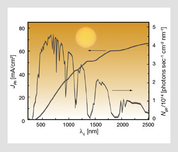
Spectral photon flux for standard illumination conditions of Air Mass (AM) 1.5 G at 1 sun (corresponding to an integrated intensity of 100 mW/cm2) and the corresponding photocurrent density JPh available for a device that would harvest all the photons contained in the spectral interval [0, λc] with a conversion efficiency of unity (ASTM E892-82).
Therefore, the performance of PV cells and modules is reported for standard test conditions of 1 kW/m2 (also called 1 sun) at a temperature of 25° C, and for a solar reference spectrum AM 1.5.
AM n stands for “Air Mass n,” in which n is the ratio of any path length through the atmosphere to its minimum. Therefore, n=0 refers to conditions outside the atmosphere, and n=1/cos q, otherwise. The figure on the facing page shows the spectral photon flux for standard illumination conditions of AM 1.5 G at 1 sun. AM 1.5 G is defined as the standardized spectral irradiance distribution of the sunlight incident on a flat surface tilted at an angle of 37° with the sun at a zenith angle of 48.19°. G stands for “global” spectrum, which includes diffuse as well as direct light, and q is the zenith angle.
The average energy produced per day by a PV system is then a function of the insolation (a measure of solar radiation energy incident on a surface), which varies with geographical location, and given by the product of the power generation capacity and the average number of hours of irradiance at 1 sun.
For instance, in the state of Georgia, the average daily insolation is 4.5 hours per day, which translates into 135 kWh of energy generated each month per kW of power capacity. With solar modules that have a power conversion efficiency of 10 percent, a PV system will have a power capacity of 1 kW for each 10 m2 of active light harvesting area.
 Average insolation map of the United States
The growth of the PV industry is generally measured in newly installed electrical power generation capacity and has been recorded since 1993, when the IEA was established. In 2005, for the first time in history, a total of more than 1 GW of power capacity was added, increasing the cumulative installed capacity by 42 percent and reaching a value of 3.7 GW in the IEA PVPS countries (90 percent of the worldwide production). The greatest proportion was installed by Germany and Japan alone (85 percent).
This 42 percent annual growth rate of cumulative installed capacity has been fairly steady in recent years and has been accompanied by a steady decrease in the price of solar modules, from nearly $100 in 1976 down to an average of $4 (per watt). This trend is often referred to as the learning curve.
However, in recent years, the decrease of module cost has been leveling off—a trend that has been attributed to tight supplies of Si feedstock. This has been considered a limitation for the future expansion of the PV industry, since 94 percent of the modules produced by the countries that report to the IEA were based on crystalline silicon technologies in 2005. However, with new silicon feedstock production lines becoming operational soon, this shortage will most likely not last and the module costs will continue to decrease.
Crystalline Si PV modules are fabricated from three kinds of ingots and wafers: single crystal ingots; multicrystalline ingots; and multicrystalline ribbons. Ingots are cut into blocks and then sawn into thin wafers, whereas ribbons are cut into wafers directly. Until 2000, the main source of wafers for the PV industry was rejects from the semiconductor industry.
However, since then, with the important growth of the PV industry, virgin silicon has become the main feedstock. Research and development efforts focus on replacing expensive chemical gaseous purification methods of Si by lower-cost processes in the condensed phase. Worldwide, the total production capacity of Si is estimated to be about 36,000 metric tons, of which one-half is used by the PV industry. Another trend is to decrease the wafer thickness, which is motivated by the rising price and supply shortening of the Si feedstock.
Japan is a leading producer of PV supplies. The country accounted for 55 percent of PV cells and 50 percent of PV modules for all the countries reporting production to the IEA in 2005. Germany was in second place, with 23 percent and 18 percent of cells and modules, respectively. The largest producers in Japan are Sharp (28 percent), Kyocera (9 percent) and Sanyo Electric (8 percent), while Q-Cells is the largest producer in Germany (11 percent).
Worldwide, the photovoltaic industry employs about 55,000 people, and its business is growing annually by 30 percent. Public budgets for market simulation, research and development, demonstrations and field trials reached around $1 billion worldwide in 2005.
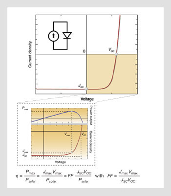 (Top) Electrical characteristics and idealized equivalent circuit for a solar cell, and definition of the open circuit voltage VOC and the short-circuit current JSC. (Bottom) Close-up of the fourth quadrant and illustration of the point of maximum power.
Metrics for solar cells
In their simplest form, the electrical characteristics of photovoltaic devices can be modeled by a diode and a current source connected in parallel, where the current source describes the process in which the solar cell converts the sunlight, or optical power, directly into electrical power.
Unlike photodetectors that operate in reverse bias, photovoltaic cells operate in the fourth quadrant of the current-voltage characteristic graph, where the voltage is positive and the current density negative. When the device is under illumination, two quantities can be easily determined experimentally: the intersects of the electrical characteristics with the vertical and horizontal axes, which correspond to the short-circuit current density (JSC) and the open-circuit voltage (VOC).
At any point on the electrical characteristic in the fourth quadrant, the solar cell produces an electrical power density that is given by the product of the voltage and the current density. This product is maximized at a point that corresponds to a voltage Vmax and a current density Jmax, which is the point of maximum power. The power conversion efficiency η, which is the most important metric for a PV cell, is then defined as the power density produced at the point of maximum power divided by the incident optical power density. The cell is combined with a matched load to operate at the maximum power condition. Power conversion efficiency η is often also defined as a function of a fill factor (FF) and given then by the product FF JSC VOC divided by the incident optical power density. FF is then a measure of how rectangular or how rectifying the current-voltage characteristic is.
Classification of solar cells and technological trends
Today, photovoltaic technologies are dominated by wafer-based crystalline silicon (monocrystalline, polycrystalline and ribbon silicon), which are often referred to as first-generation devices. The major driver for research and development on PV cells during the past 30 years has been to reduce the cost of PV-generated electricity (currently $0.30-$0.50/kWh) and make it competitive with that of electricity produced by conventional coal-firing plants (national average $0.08-$0.1/kWh).
The cost of electricity produced by a solar cell or module is primarily influenced by the interplay between its operational lifetime, its manufacturing cost per unit area and the power conversion efficiency. Therefore, ongoing research efforts are focused on further increasing the efficiency of silicon-based solar cells with different grades of silicon that can be manufactured at lower cost. The most efficient crystalline silicon solar cells to date were developed at the University of New South Wales and have a power conversion efficiency of 24.7 percent.
However, the high number of steps required in the fabrication of these PERL (passivated emitter, rear locally diffused) devices do not make them compatible with low-cost manufacturing. In June 2007, Sanyo Electric Co. Ltd. reported crystalline silicon cells with 22 percent efficiency that can be manufactured. Likewise, Mitsubishi Electric Corporation announced in May 2007 that it has demonstrated multicrystalline silicon cells with 18 percent efficiency. Despite these constant improvements in bulk crystalline technologies, alternative photovoltaic approaches have been developed simultaneously during the past few decades.
In an effort to reduce manufacturing costs, thin film technologies that require less materials and can be processed onto thin and lower-cost substrates (e.g., glass) using high throughput fabrication have been the subject of active research and development. These thin-film technologies, also referred to as second-generation devices, are based on light absorbing materials such as amorphous silicon, polycrystalline/amorphous silicon combinations, chalcogenide-based thin films (e.g., CuInSe2 or CIS, CuInGaSe2 or CIGS) and II-VI semiconductors (CdTe, CdSe, paired with CdS).
Despite remarkable progress with the demonstration of CIS and CdTe laboratory cells with 19.5 and 16.5 percent power conversion efficiencies, respectively, these second-generation technologies still have a modest market share. Nevertheless, several companies are engaged in their manufacture, including Shell Solar (United States) and Wurth Solar (Germany) for CIS, Global Solar and Miasolé (United States) for CIGS, and First Solar (United States) for CdTe.
Third-generation approaches include multijunction cells that are comprised of multiple inorganic semiconductors with different bandgaps to harvest a larger portion of the solar spectrum, and other approaches that do not rely on conventional single p-n junctions of inorganic semiconductors, such as quantum dot photovoltaic cells and organic photovoltaics.
Organic photovoltaic devices
Organic or organic-based PV devices can be classified in several ways. First, one has to distinguish solid-state approaches from dye-sensitized solar cells, which are electrochemical cells that require an electrolyte. The latter cells, developed by Prof. Grätzel at EPFL in Lausanne, have demonstrated efficiencies of 10 percent in laboratory cells containing liquid electrolytes (J. Am. Chem. Soc. 115, 6382).
Dye-sensitized solar cells (DSSCs) based on gel electrolytes have lower efficiencies. Nevertheless, several companies have engaged in their manufacture, including G24 Innovations, a British company located in a 187,000 sq ft. plant set over 23 acres to produce DSSCs on a commercial scale. The challenges involved in the manufacture of DSSCs have driven intensive research and development into all-solid-state approaches.
After the seminal work of C. Tang at Kodak in the 1980s, which led to the demonstration of thin-film molecular solar cells with power conversion efficiencies close to 1 percent, current small-area laboratory cells have reached power conversion efficiencies of 3 to 6 percent and have the potential to reach 15 percent. They can be divided into three categories: small molecule multilayer devices; polymeric mixtures; and hybrid organic/inorganic semiconductor nanostructure blends.
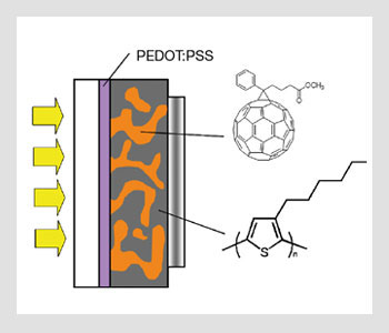 The geometry of bulk heterojunction solar cells. PEDOT:PSS stands for poly(3,4-ethylenedioxythiophene) poly(styrenesulfonate); it is an intrinsically conducting polymer used to modify the ITO electrode.
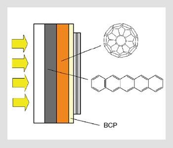 Multilayer heterojunction solar cells. BCP, or bathocuproine, is used as a passivation and electron transport layer in multilayer devices.
OPV device technologies have the following attributes:
• the component organic materials can be processed from the vapor phase or from solution at low temperatures;
• the materials can potentially be processed into large-area devices at low cost;
• OPV cells can be intrinsically lightweight and shatterproof;
• the high absorption coefficient of organic materials can reduce the thickness needed to absorb light efficiently, reducing the amount of material needed; and
• OPVs are amenable to patterning and processing using soft lithography, printing and embossing, which should further lower the cost of module manufacturing.
Technologies combining these properties are anticipated to pave the way toward low-cost, lightweight, large-area, flexible and conformable solar panels. Their manufacturing costs will likely be far lower than those of conventional Si-based photovoltaic technologies. The ultimate goal is to develop materials that can be processed into cells by a roll-to-roll process involving printing.
Such cells may find applications in on-grid power generation by 2015, and in numerous off-grid applications to power the ever-increasing number of portable electronic digital devices and sensors in the near term. Electrical energy provided by paper-thin solar cells will be essential to power the wide range of new devices and circuits, including radio-frequency identification tags (RFID) and smart sensors that are used for environmental and structural monitoring. Such wireless sensing systems can be used for building automation for energy management.
Organic semiconductors and organic photoconductors
Except for dye-sensitized Grätzel cells, the fabrication of most organic solar cells is based on organic/organic heterojunctions formed between hole-transporting (donor-like) and electron-transporting (acceptor-like) molecules, polymers or semiconductor nanostructures. These junctions can be formed in multilayer devices or by blending, leading to bulk heterojunctions. The organic materials are usually sandwiched between a transparent electrode such as indium tin oxide and a metal electrode. Some of these device geometries are illustrated in the figures above.
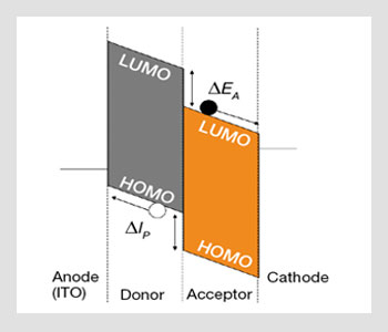 Energy-level diagram of organic solar cells. LUMO is for lowest (energy) unoccupied molecular orbital and HOMO is the highest occupied molecular orbital. ΔEA is the difference in electron affinity between the two compounds; ΔIP is the difference in ionization potential. The full and open circles represent electrons and hole, respectively.
Unlike inorganic crystals such as Si, organic materials have a low dielectric constant, which leads to a strong Coulomb interaction between the hole and the electron created after absorption of a photon. As a result, excitons with binding energies larger than a kT (roughly 500 meV to be compared with 26 meV) are formed at room temperature. In order to contribute to the photocurrent, these excitons must dissociate at the heterojunctions formed between the donor- and acceptor-like materials.
Efficient carrier generation is then achieved at the donor/acceptor heterojunction via photoinduced charge-transfer reaction when the relative energies of the HOMO (highest occupied molecular orbital) and LUMO (lowest unoccupied molecular orbital) levels are chosen to allow for energy offsets greater than the exciton binding energy.
Only the excitons that can diffuse to that interface will dissociate into electron/hole pairs efficiently. Thus, it is important to use materials with large excitonic diffusion lengths. The thickness of the layers cannot exceed this excitonic diffusion length, but at the same time the layers must be thick enough to absorb most of the incident radiation. This limitation is often referred to as the excitonic bottleneck. However, it can be overcome by optimizing the figure of merit αL, where α is the absorption coefficient and L the excitonic diffusion length. The steps involved in the photogeneration process are shown in the figure below.
If the excitonic diffusion length is a limiting factor for a given set of donor- and acceptor-like materials, an alternative is to mix these compounds and create an interpenetrated network with nanoscale domain sizes. In this case, the solar cell is comprised of a single layer sandwiched between electrodes instead of two layers of neat films of a donor and an acceptor material. These single-layer devices based on blends are often referred to as bulk heterojunctions. This is because an exciton created inside the film will always be in proximity to a heterojunction within the nanoscale interpenetrated network where it can dissociate efficiently into an electron-hole pair.
An advantage of the bulk heterojunction geometry is that you can mix donor- and acceptor-like materials into a blend from solution and coat it into a single film. In contrast, in the bilayer geometry, it can be difficult to coat several layers on top of one another when using materials processed from solution.
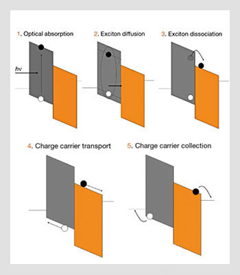 Physical processes involved in the operation of multilayer organic photovoltaic cells. Full and open circles represent electrons and hole, respectively.
However, an intrinsic challenge of this approach is how to control the structure of the phase separation of the blend needed to generate conduction paths in the donor- and acceptor-like materials for the holes and electrons, respectively. These carriers result from the photodissociation of excitons at the high-surface-area heterojunctions formed in the blend. The carrier mobility in these conduction paths must be sufficient to ensure that the electron and hole carrier diffusion lengths are larger than the thickness of the film, which is typically in the range of 100 to 200 nm.
Since organic solar cells are composed of several thin-film layers formed from materials with different optical properties, mismatch of the complex refractive index at these multiple interfaces leads to multiple reflections that produce optical interference effects. As a result, the light distribution inside the solar cell is highly inhomogeneous, and determined by a complicated interplay among the relative optical constants of the materials and their thickness. Optical constants for these layers must be measured precisely using frequency-resolved ellipsometry experiments in order to develop reliable design tools to optimize the thicknesses of the different layers.
In multilayer devices fabricated by vapor deposition, hole-transport layers are mainly composed of phthalocyanines (e.g., Cu-PC, Zn-PC) or oligoacenes (e.g., tetracene, pentacene). Electron-transport layers are made from fullerenes (e.g., C60 and C70) or perylene tetracarboxylic derivatives. In polymeric bulk heterojunctions, most of the studies have been devoted to mixtures of polyphenylene vinylene or polythiophene derivatives, and soluble substituted fullerenes PCBM-C60 and PCBM-C70.
These materials harvest the visible part of the solar spectrum quite well. Peak external quantum efficiency of 80 percent can be achieved, leading to power conversion efficiencies of 4 to 5 percent. Current efforts are geared toward developing new materials that are sensitive in the near infrared part of the spectrum.
With the availability of new materials that absorb in complementary parts of the solar spectrum, the power conversion efficiency can be further improved by designing multijunction devices in which two heterojunctions are formed on top of one another. Such tandem cells have been demonstrated recently with both small molecules processed from the vapor phase and by using materials processed from solution.
Alan Heeger’s group at the University of California at Santa Barbara (UCSB) in collaboration with the Gwangju Institute of Science and Technology (GIST, Korea) recently demonstrated tandem cells with efficiencies larger than 6 percent in small-area (0.045 cm2) laboratory cells (Science, 317, 222). However, the long-term stability of these cells remains elusive. Nevertheless, researchers are making continuous progress in improving the stability of organic semiconductors and developing new low temperature packaging technologies.
Outlook
Scientists and engineers are likely to use sophisticated quantum-chemical modeling tools to develop next-generation molecules and polymers with improved properties. Advances in nanotechnology will lead to new conducting inks and transparent electrodes, which can be printed at low cost onto large-area flexible substrates.
However, before these potentially disruptive devices reach the market, much work remains to be done to scale the size of these devices up while maintaining high efficiencies and demonstrating shelf lives of several years and long-term stability under constant illumination. Like other printable optoelectronic technologies, such as organic light-emitting devices for displays or solid-state lighting, organic photovoltaic devices are more likely to be fabricated on glass substrates in the near term because glass is a stable and efficient barrier for water and oxygen using batch processing.
However, we envision that manufacturing using roll-to-roll processing will eventually be possible, as new advances are made in flexible barrier coating technologies and flexible transparent conducting electrodes.
Organic photovoltaics holds promise as a cost-competitive and flexible renewable energy source, as long as research and development resources continue to be made available. With efficiencies constantly increasing, the future of organic photovoltaic technologies looks bright.
[ Bernard Kippelen is a professor at the School of Electrical and Computer Engineering at the Georgia Institute of Technology. He serves as the associate director of the Center for Organic Photonics and Electronics and the NSF-funded Science and Technology Center MDITR. He is an OSA Fellow. ]
References and Resources
>> International Energy Agency Photovoltaic Power Systems Program
>> C.W. Tang. Appl. Phys. Lett. 48, 183 (1986).
>> S.S. Sun and N.S. Sariciftci. Organic Photovoltaics: Mechanisms, Materials and Devices. Taylor and Francis, Boca Raton, Fla. (2005).
>> M.K. Nazeeruddin et al. J. Am. Chem. Soc. 115, 6382 (1993).
>> J.Y. Kim et al. Science 317, 222 (2007).

