

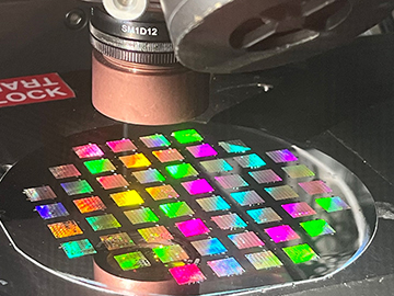
Researchers in Switzerland, China and Russia have fabricated wafers containing 1 cm2 chips, each made up of 49 novel silicon metasurfaces to modulate infrared laser light. [Image: EPFL BIOS CC BY SA 4.0]
An international group of scientists has developed a new type of silicon-based metasurface that can modulate mid-infrared light at very high speeds while achieving both high precision and large amplitudes (Nat. Commun., doi: 10.1038/s41467-026-75121-6). They reckon that their system, which is compatible with CMOS fabrication, could find application in everything from telecommunications to quantum optics.
Creating the right metasurface
Metasurfaces are extremely thin artificial materials made up of arrays of sub-wavelength-sized features that can manipulate the phase, amplitude and polarization of light in novel ways. They are especially useful when exhibiting sharp resonances—quantified by the dimensionless parameter known as the quality (Q) factor—since their narrowband response and strong enhancement of electromagnetic fields can enable efficient lasing, high-resolution spectroscopy and other applications.
However, it is no mean feat to create a metasurface that combines a high Q-factor with a significant amplitude contrast. It is also difficult to build a device whose optical response can be actively controlled in time. These problems are particularly acute for metasurfaces at mid-infrared wavelengths, of the order of a few micrometers, since loss becomes significant. The materials typically used for telecoms, for example—silicon-on-insulator or silicon-on-sapphire—experience major absorption when operated at slightly longer wavelengths.
In the latest work, Hatice Altug, Felix Ulrich Brikh and colleagues at the EPFL in Lausanne, Switzerland, working with researchers in Russia and China, show how these problems can be overcome by using metasurfaces made from suspended single-crystalline silicon membranes compatible with high-throughput wafer production. They fabricated the membranes by selectively removing (infrared-lossy) buffer oxide from silicon-on-insulator wafers and etching windows through the carrier silicon, while tailoring membranes’ resonance for the mid-infrared by patterning them with a hexagonal lattice of elliptical holes.
Putting it to the test
The researchers first assessed the static performance of their system by using a custom-made microscope to measure the transmission spectrum from a range of designs made using both chip-scale ebeam lithography and wafer-scale deep-UV lithography. They varied the ellipticity of the holes from one metasurface to the next, recording the tradeoff between Q-factor and resonance amplitude in each case. For circular holes distorted by a factor of 1.08 they achieved a Q-factor just below 3000 and an amplitude contrast of over 50%—a combination that they say "represents a major improvement over the previously reported mid-IR metasurfaces."
After this, Altug and colleagues switched their attention to dynamic tests, using two different approaches to tune the metasurfaces' response to mid-IR radiation. One of these involved evaporating thin films of aluminium onto the edges of each metasurface to drive an electrical current through the structure, so heating it up and modifying its refractive index through the thermo-optic effect. They doped the silicon with phosphorous to enhance heating at a given voltage, but only insofar as they could maintain a high Q-factor by minimizing non-radiative optical losses.
To maximize the speed of metasurfaces' response they had to overcome the fact that air is a poor thermal conductor, making it a struggle to remove the heat from one cycle before beginning the next. The trick here was to fabricate smaller membranes, since these can dissipate heat more efficiently from their sides than larger versions can. However, they had to retain a certain number of unit cells within the array to keep the Q-factor high. They found they could achieve the necessary sharp resonance for membranes as small as 75 micrometers, which expelled heat quickly enough to reach a modulation frequency of 14.5 kHz.
An all-optical scheme
This speed, however, was dwarfed by that obtained in the researchers' second (all-optical) modulation scheme. This involved directing visible pump pulses at the silicon membrane, which generated charge carriers within the silicon that altered its refractive index on extremely short timescales. To probe these fleeting modifications, they used a second source of pulses in the mid-infrared, varying the time delay between the two sets of pulses to establish how long it took the material to recover its original resonance after being shifted to slightly shorter wavelengths by the visible laser.
They found they could change the metasurface and bring it back to its original state in as little as 2 nanoseconds. While this timescale in principle sets the modulation speed, any working device would also have to dissipate the heat from the laser during each cycle. Because silicon's refractive index can be changed significantly by quite modest amounts of induced charge, so minimizing the required pump intensities, they calculated that the material should be able to cope with cycle rates as high as 120 megahertz.
Altug and coworkers say that this rate could in principle be pushed as high as 1 GHz by adding more defects to a membrane to stimulate recombination of charge carriers. However, they caution that it will not be easy to integrate an external pump laser into a practical device, making the all-optical approach harder to realize in practice than its electro-thermal counterpart. As to the fragility of the suspended membranes, they claim that structures optimized for the mid-infrared would be about as robust as widely commercialized micro-electromechanical systems (MEMS).
If the various hurdles can be overcome, the researchers believe their technology could be well-suited to a range of applications. These include free-space communication at high speeds and low powers, as well as very sensitive chemical and biological sensors and a number of enhanced capabilities in quantum optics—such as more efficient control of single-photon sources and tuneable generators of entangled photon pairs.
