
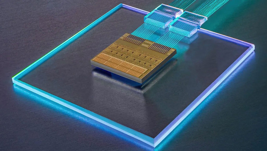
Artist view of a 4-Tbps optical I/O system demonstrated by Ayar Labs at OFC 2023, which includes two of the company’s SuperNova light sources attached to its TeraPHY “chiplets.” [Image: Ayar Labs] [Enlarge image]
On 24 May, Ayar Labs, an early-stage Silicon Valley–based developer of optical-interconnect “chiplets” and light sources for high-performance computing (HPC) and AI, announced a US$25 million increase in its Series C funding. The new Series C1 up-round—which the company characterized as “oversubscribed”—came from a group including both existing and new investors. The extra cash brought the total value of Ayar’s Series C raise, begun in late April 2022, to US$155 million.
In a press release accompanying the announcement, Ayar said it would use the added funding to “accelerate the implementation and commercialization of its optical I/O [input/output] solutions,” especially for the markets promised by generative-AI technology. The company’s CEO, Charles Wuischpard, called the new infusion of financing “further validation of our technology and plan to bring silicon photonics–based interconnect solutions to market at scale.”
Of particular interest was the participation in the up-round of Nvidia, the chip-making giant behind the graphic processing units (GPUs) and other systems empowering the recent surge in AI development.
Attacking the bandwidth–distance bottleneck
In an interview with OPN last year, Ayar Labs cofounder and chief technology officer Mark Wade described the company’s focus as “optically enabled computing.” In particular, Ayar has been designing and building silicon photonic systems that can help optically move the massive amounts of data that flow between electronic application-specific integrated circuits (ASICs) in HPC and AI applications.
Replacing electronic I/O with optical I/O in these systems targets the so-called bandwidth–distance bottleneck in HPC and AI, data centers and other settings. In principle, moving as much data as possible, as for long a distance as possible, with photons in fiber rather than with electrons in copper wire should enable substantial reductions in power, operating cost and latency. Ayar’s approach to achieving those gains is, in Wade’s words, to “really push the electrical-to-optical conversion as close to the host ASIC as possible.”
Lasers and chiplets
Ayar has two CMOS-native product lines addressing the HPC and AI computing markets. One is a chip-scale laser light source called SuperNova. The other, dubbed TeraPHY, is an optical I/O “chiplet” that can be flip-chip bonded to the same substrate as an electronic ASIC and sit immediately adjacent to it.
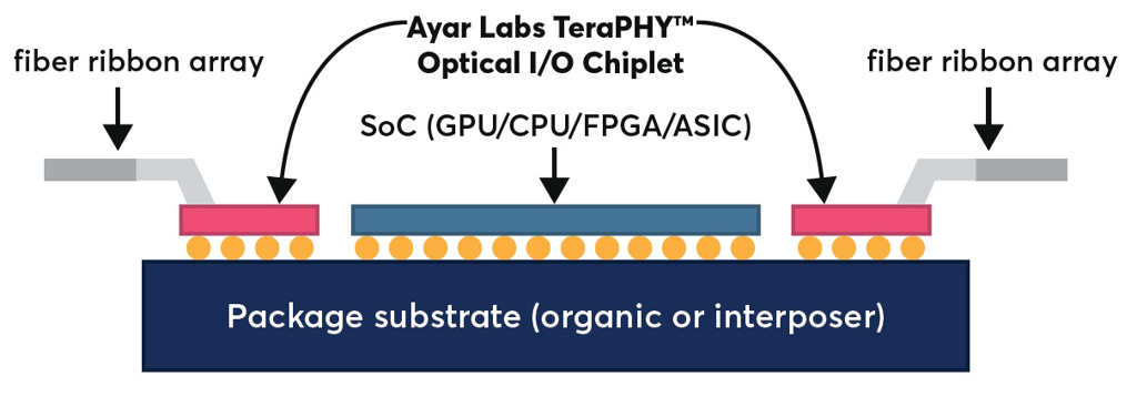
Ayar’s TeraPHY chiplets are designed to be flip-chip bonded onto the same substrate as the ASIC to simplify integration. [Image: Ayar Labs technical brief, 2021] [Enlarge image]
This architecture enables the volumes of data coming out of the ASIC to be converted to the optical domain as quickly as possible, without the need to travel through copper wires. Further, according to Wade, the microring-resonator system handling the electrical-to-optical conversion in the chiplet allows the conversion to take place “at a starting point that’s much denser, and ultimately much more energy efficient,” than traditional pluggable transceivers.
At the 2023 OFC Conference this past March, Ayar demonstrated what it called “the industry’s first 4 terabit-per-second bidirectional wavelength-division multiplexing optical solution.” The demo system moved 64 wavelengths of mulitplexed light from one of Ayar’s SuperNova sources through eight fiber links between two TeraPHY chiplets, at 2.048 Tbps in each direction, for 4.096 Tbps of bidirectional bandwidth. And the data transfer is highly energy efficient, according to Ayar, requiring less than 5 pJ per bit.
The Nvidia factor
The recently announced US$25 million Series C1 up-round, which was led by a new participant, the investment group Capital TEN, also included new and existing investment firms and strategic partners such as Nvidia, Applied Ventures, Global Foundries HP and Lockheed Martin.
The funding from Nvidia—which also participated in the original US$130 million Series C raise last year—looks particularly interesting, and timely.
The funding from Nvidia—which also participated in the original US$130 million Series C raise last year—looks particularly interesting, and timely. As has been widely reported, the US chipmaker said on 24 May (the same day as Ayar’s announcement) that it expects revenues for its July quarter to reach US$11 billion, more than 50% ahead of analysts’ previous expectations. The company’s stock price soared some 27% the day of the news, swelling Nvidia’s market capitalization by some US$184 billion—said to be the biggest one-day rise in the market’s history.
Behind both the gain in projected revenue and the skyrocketing market value is Nvidia’s pole position as high-end chip supplier to the burgeoning generative-AI area. The company’s powerful H100 processor, a US$40,000 chip specifically targeting generative-AI applications, has sold at a blistering pace since the unveiling of OpenAI’s ChatGPT in November 2022.
The much-publicized OpenAI chatbot, Nvidia CEO Jensen Huang recently told the Financial Times, “created instant demand” for the H100 processor, especially among cloud-computing providers such as Amazon and Microsoft. At a recent Wall Street Journal event, Elon Musk, who is launching a new generative-AI startup of his own called X.ai, quipped that Nvidia GPUs “are considerably harder to get than drugs.”
“Generative AI models with trillions of parameters are accelerating demand for this platform,” said Craig Thompson, the vice president for business development at Nvidia’s Networking Business unit. And that, he maintained, “is why we are increasing our investment in Ayar Labs.”
