
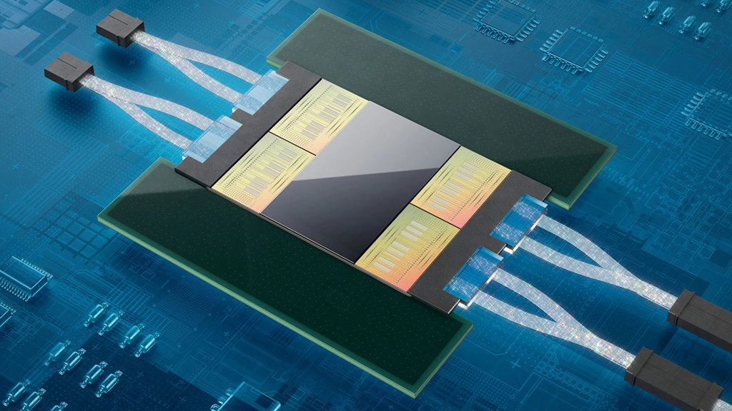
Ayar Labs’ optical I/O “chiplets” (gold) are designed to place optical-to-electrical/electrical-to-optical conversion right next to an application-specific integrated circuit (gray), such as an Nvidia GPU—thereby keeping the data in the less-power-hungry, higher-bandwidth optical domain as long as possible. [Image: Ayar Labs] [Enlarge image]
As the dreams of artificial intelligence and machine-learning system developers have grown ever larger, the suppliers of hardware to enable those systems have started to bump up against some fundamental constraints. For example, Nvidia—a leader in graphics processing units (GPUs) that do the heavy lifting for a wide range of computationally intense systems such as those in AI—believes that, by 2023, advanced AI models could entail 100 trillion or more connections, rivaling the number of synapses in the human brain.
Those kinds of numbers, which far outstrip what can be handled a single processor, will require massive amounts of data to flow rapidly from one application-specific integrated circuit (ASIC) to another within data centers. Much of that chip-to-chip communication still takes place via copper interconnects in the electrical domain. And shunting around those immense data volumes will consume large, perhaps cost-prohibitive amounts of power.
One company seeking to help solve that problem is the Silicon Valley-based Ayar Labs, which is developing a line of CMOS-friendly, low-power optical input/output (I/O) products to feed the market for interconnects in high-performance computing and AI. Nvidia seems to find the approach promising. On 25 May, Ayar and Nvidia announced that they were collaborating on “integrating Ayar Labs’ technology to develop scale-out architectures enabled by high-bandwidth, low-latency and ultra-low-power optical-based interconnects for future Nvidia products.”
A focus on the interconnects
A number of early-stage and startup companies are working to carve out a place for photonics in aspects of AI and high-performance computing. Some, such as Lightelligence and Lightmatter, are developing “AI accelerator” chips—intricate next-gen photonic integrated circuits that tackle, entirely in the optical domain, the power-hungry, repeated matrix multiplications required by AI computing. But Mark Wade, an Ayar Labs cofounder and the firm’s CTO, stresses that’s not what his company is about.
“It’s an important distinction to say that we are not doing that,” he told OPN. Instead of optical computing, according to Wade, Ayar focuses on “optically enabled computing”—and, in particular, on solving the bandwidth–distance bottleneck increasingly faced by traditional computer architectures relying on electronic host ASICs.
As computing demands have mushroomed, Wade says, “the trend has been that these ASICs have been trying to move more and more bandwidth between different packages.” And, while a lot of the communication within data centers happens in the optical domain, much of the package-to-package communication is still done electrically along copper interconnects. That sets up a trade-off: The more copper and the greater the I/O distance in the electrical domain, the less bandwidth can flow from chip to chip with sufficiently low latency and power requirements.
TeraPHY and SuperNova
Ayar Labs aims to break that bottleneck, Wade says, through “a new class of photonic integration and technologies and products” that “really push the electrical-to-optical conversion as close to the host ASIC as possible.”
The Ayar chiplets are designed to be flip-chip bonded onto the same substrate as the ASIC to simplify integration. [Image: Ayar Labs technical brief, 2021] [Enlarge image]
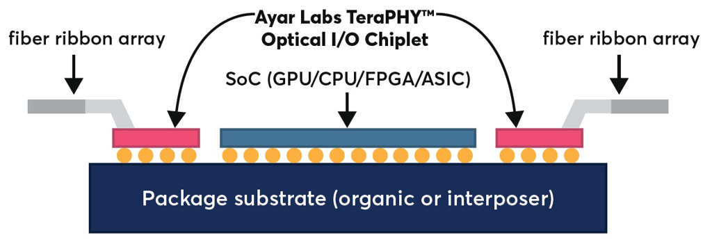
One element of this is an optical I/O “chiplet” called TeraPHY (yes, it’s pronounced “terrify”). The chiplet is designed to be flip-chip bonded to the same substrate as an ASIC (such as an Nvidia GPU) and sit directly next to it. Data-carrying light is fed, via a ribbon of single-mode fiber connections, into (or out of) the chiplet, where a system of microring resonators decodes the light signal into an electrical one (or vice versa).
“The whole point,” says Wade, “is to take the high bandwidth coming out of the host SoC [system on chip], convert it to the optical domain as fast as possible, and then have a much more scalable way to move massive amounts of bandwidth with low energy [over] long distances.” And, he adds, the level of miniaturization and integration enabled by the microring-resonator architecture enables the optical-to-electrical/electrical-to-optical conversion to happen “at a starting point that’s much denser, and ultimately much more energy efficient,” than traditional products, like pluggable transceivers, that are aimed at the more mature optical-communications market.
The other core component of Ayar’s system is the company’s SuperNova laser light source, which sits on a different chip and can produce 16 wavelengths of light delivered into 16 fibers (each of which can itself carry up to 16 wavelengths). This disaggregates the light source from the ASIC package, which the company believes affords more flexible deployment across applications and easier replaceability of parts in the field.
“Massive” market opportunity
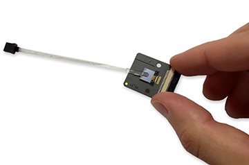
The company’s laser light source, SuperNova. [Image: Ayar Labs]
The partnership with Nvidia is only one of a flurry of announcements that have come from Ayar Labs in the past few months. An earlier announcement, in February 2022, unveiled a strategic collaboration between Ayar and Hewlett Packard Enterprise (HPE) to develop “silicon photonics solutions based on optical I/O technology.”
Subsequently, in late April, Ayar Labs reported that it had snagged US$130 million in Series C funding from an investor group that included HPE, Nvidia, Intel, Global Foundries and a variety of venture-capital partners. That chunk of cash, Wade told OPN, will be used for “maturing our commercial operations, our manufacturing and supply-chain operations, our qualification cycles, and really setting the stage to build a company that can deliver millions of these parts to multiple market segments.”
This year the numbers will be smaller; Ayar Labs expects to ship thousands of units to early-stage customers in 2022. “That’s not yet massive volume,” Wade acknowledges. “But our ability to deliver thousands of units sets the stage for how we plan to scale into the future.”
And Wade—who has been “working on this technology for more than a decade now, and working on commercializing it in our labs for the last five or six years”—firmly believes that the demand will be there.
“This solution that we’re building is not a niche solution that’s targeting one market segment,” he maintains. “It’s actually going to be a ubiquitous problem that that multiple market segments and customers start facing. And we think the overall market opportunity there, as we go into the middle and second half of this decade, is truly massive.”
