
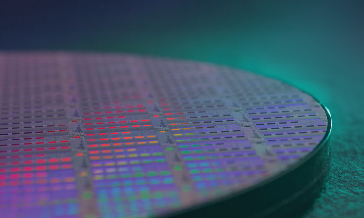
 A wafer of the TeraPHY optical I/O “chiplets” being developed and marketed by the US-based company Ayar Labs. [Ayar Labs]
For decades, Moore’s law has held sway in the semiconductor industry, with the number of transistors in each microchip doubling about every two years. But when it comes to the energy consumption of those chips, progress has started to break down. Previously, the energy per logic operation fell rapidly with each new generation of chips. Now the trend is flat or only slightly downward, leading to much lower gains in performance.
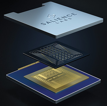 Salience Labs, a spin-out from the Oxford University, UK, lab of Harish Bhaskaran, is working toward commercialization of hybrid electronic–photonic chips for AI applications. [Salience Labs]
This energy problem is becoming more urgent thanks to the extraordinary rise in artificial intelligence, now used in everything from internet searches and language translation to image recognition and self-driving cars. Tech companies such as Google have devised ways to make digital AI computations more efficient. But some experts reckon that demand for processing will become so acute as to require a whole new technology: photonic computing.
Rather than encoding and manipulating data by packaging electrical currents into 0s and 1s, photonic computers rely on the physical, analog properties of light. Data are typically represented as variations in the amplitude or phase of a laser beam, and are processed as the beam propagates across a suitably initiated series of optical components. This all takes place at light speed and consumes no more energy than what’s needed to power the laser source—both the processing time and the energy requirement being independent of the input size.
Until fairly recently, work on photonic computers was confined largely to bulky laboratory experiments. But integrated photonics has changed that, making it much easier to scale up such technology and opening the door to commercial products. The result has been the creation of some dozen start-up companies, raising the prospect that, after decades of frustration, optical technology might finally challenge the mighty transistor.
Until fairly recently, work on photonic computers was confined largely to bulky laboratory experiments. But integrated photonics has changed that.
Those companies have raised hundreds of millions of dollars between them, hired some of the brightest minds in photonics and computing, and formed partnerships with leading multinationals. While some may ultimately not survive, Harish Bhaskaran—an engineer at Oxford University, UK, and founder of the university spin-off Salience Labs—says each is trying to address a slightly different part of what is potentially a huge market. “This is such a large space that there is enough room for many companies,” he says.
Nature’s computations
When scientists embarked on research into optical computing back in the 1960s, their aim was to build devices dedicated to quite specific tasks. In particular, they looked to exploit the fact that the image formed by a coherent light beam passing through a lens is the Fourier transform of the input field. Devices known as optical correlators employed two spatial light modulators and two lenses to compare the Fourier transform from an input signal with a predefined optical filter. This could in principle enable target recognition and signal processing for synthetic aperture radar, for example.
Securing data with light
Fully homomorphic encryption (FHE) allows sensitive data to be processed while remaining encrypted, so that even the processing hardware has no access to them. It involves adding random noise during the encryption procedure, but relies on multiplying high-order polynomials to keep the noise in check. These complex calculations require roughly a million-fold increase in the number of operations compared with unencrypted processing, making them untenable on standard digital computers. But they can be drastically simplified if the data are first subject to a Fourier transform, and then re-converted via a second transform.
Optalysys does this by encoding data in tiny laser beamlets that it passes through a diffraction grating etched onto a piece of silicon, to create a Fourier transform of the input data stream. Joseph Wilson, the company’s head of applications, says this arrangement is far more suited than bulk optics for converting electrical signals into optical and vice-versa. “Optics offers you two paths, either you go really big or really fast,” he says. “We have now chosen the latter.”
Company director Nick New says that the firm, set up in 2013 and based in Leeds, has so far raised about £10 million (some US$11.5 million) and is currently testing its first chips in the lab. After integrating the necessary electronics over the next 18 months, he predicts that these devices should be about 500 times faster than the best electronic-only chips. If all goes well, he adds, the product should appear on the market in 2025.
The Enable chip, described by its maker Optalysys as the “complete solution for FHE.” [J. Wilson]
A number of companies have been set up to try and commercialize such technology. Some have folded, while others have evolved. In 2001, engineer Nick New founded Cambridge Correlators in the United Kingdom to market optical correlators for pattern recognition. Since then, however, he’s set up a new company called Optalysys to make products from silicon photonics and electronics. These programmable chips convert digital information into the optical domain and back again to carry out a very secure but demanding type of data encryption (see “Securing data with light,” right).
While Optalysys has given a modern twist to the well-established approach of exploiting light’s natural computations, others have attempted to make more general-purpose photonic processors. In the 1970s and 1980s, scientists started working on the optical equivalent of the transistor. But it soon became clear what a tall order that would be given photons’ lack of mutual interaction—and, therefore, their inability to carry out (nonlinear) switching. Many researchers setting up photonic-computing companies in recent years thus have instead focused on one specific but much-demanded calculation, and one that digital electronics struggles to perform—matrix multiplication, which underpins artificial neural networks.
A neural network is able to recognize certain patterns in data thanks to the weighting of links between its many artificial neurons, which are usually arranged in layers. The output of any one neuron is determined by the sum of weighted inputs from neurons in the previous layer, together with a nonlinear activation function—an arrangement that is repeated across the network and which enables the final layer to indicate whether or not a given pattern is present at the input.
The sum of weighted inputs is represented mathematically as a multiplication between a vector (the input values) and a matrix (the weights). For a digital processor this amounts to a long series of multiplications and additions, involving much back-and-forth shunting of data between memory and processors in the form of electrons travelling along wires. That takes time and generates heat. Dedicated AI chips such as Google’s Tensor Processing Unit save both time and energy by cutting back on many of the operations that take place in a general-purpose CPU and avoiding repetitious extraction of data from memory. Ultimately, however, all digital electronic chips are limited by their von Neumann architecture.
Abu Sebastian, an electrical engineer at IBM in Zurich, Switzerland, underscores this limitation by comparing such chips with one particularly efficient neural network—the one in the human brain. He points out that the brain consumes on average only around 20 W and an estimated 1 femtojoule (10–15 J) for each synaptic operation. In contrast, he says, their continuous movement of data means that digital chips based on the von Neumann architecture are likely to consume hundreds of femtojoules per operation, “even if the processor consumes almost no energy.”
Optical processors can slash the energy needed for matrix multiplications, because the non-interaction of photons makes them well suited to such linear algebra.
Constructive interference
Optical processors can slash the energy needed for matrix multiplications, because the non-interaction of photons makes them well suited to such linear algebra. Until recently, though, they were too bulky to compete with electronics. Now, as Bhaskaran points out, they too can be fabricated as chips, using CMOS processes similar to those for making conventional integrated circuits—with such fabrication offered by a number of foundries around the world. “The whole manufacturing scene has changed,” he says. “It means that if there is a market, you can make it.”
One of the first groups to investigate integrated photonics for optical computation was that of Dirk Englund and Marin Soljačić at the Massachusetts Institute of Technology (MIT), USA. The group has explored a number of different schemes, including one proposed by then–postdoctoral fellow Ryan Hamerly that uses an optical homodyne detector to multiply the intensity of laser pulses together and a capacitor to accumulate the electrically encoded result of successive multiplications. This enables low-energy matrix multiplications, but to be practical it would likely need bulk lenses as well as chip-based components.
The proposal that has attracted most attention instead involves what are known as Mach-Zehnder interferometers (MZIs). Made up of two 50:50 beam splitters and a pair of phase shifters incorporated into waveguides, these devices can rotate input vectors encoded into laser pulses and also scale those vectors if one half of their two input and output channels are blocked off. Since any matrix can be cast as a combination of two rotations and a rescaling, a suitable grid of MZIs can perform matrix multiplications on incoming light pulses.
The scheme was used to implement a two-layer neural network that could identify different vowel sounds, as reported in a Nature Photonics paper in 2017. That work has since led to the spinning off of two separate companies, both with offices in Boston, called Lightmatter and Lightelligence. But while both firms have gone on to develop chips that exploit MZIs in some way, neither has stuck to the original design.
Top of the class
Lightelligence was set up in 2017, and four years later released a chip called PACE containing about 10,000 photonic devices and a microelectronic chip providing control and memory. Co-founder and CTO Huaiyu Meng explains that the company had to break up the original single web of MZIs because it was too hard to maintain the very delicate phase states across a coherent network. Were any one interferometer to fail, he says, it would be “hard to isolate the impact.”
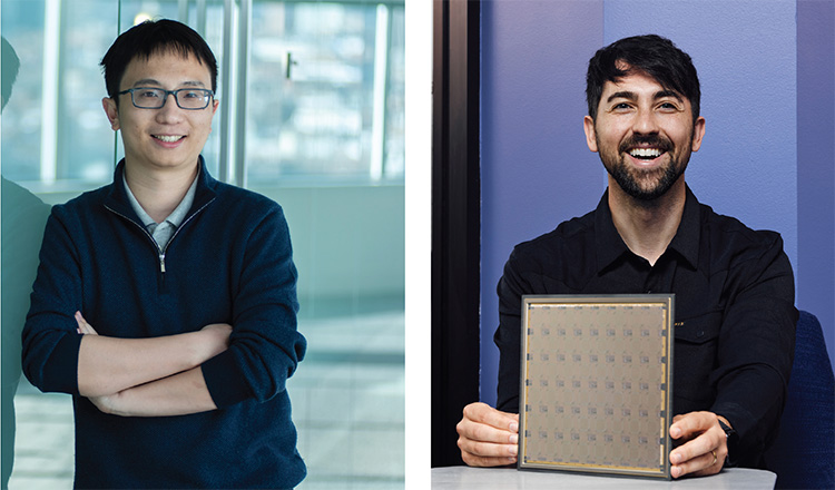 Lightelligence co-founder and CEO Yichen Shen (left) and Lightmatter co-founder and CEO Nicholas Harris (right). [D. Sella for MIT Corporate Relations / D. Levy]
Despite this limitation, says Meng, PACE is able to solve an exponentially scaling “max-cut problem” more than 100 times faster than state-of-the-art GPUs—and the company was slated to follow up with an even more powerful chip (for image recognition and object detection) at around the end of 2022. Indeed, having notched about US$200 million in investment and hired some 200 members of staff, the company’s founder and CEO Yichen Shen recently proclaimed Lightelligence to be “the leading photonic computing company in the world.”
Lightmatter’s founder and CEO Nicholas Harris begs to differ. He is skeptical about Lightelligence’s claim to have solved the max-cut problem, which, he argues, if done scalably would be “sort of like claiming you can do cold fusion.” He is reluctant to give any technical details about his own company’s new general-purpose AI chip, called Envise-beta, beyond stating that the few MZIs still in the device don’t actually do any processing. But he does say that the chip contains millions of optical components.
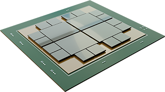
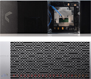 Top: The optoelectronic chip PACE from Lightelligence, released in 2021. Bottom: Lightmatter’s general-purpose AI chip Envise, the beta version of which was announced at the SuperComputing 2022 show in November. [Lightelligence / Lightmatter]
According to Harris, Lightmatter, which was founded in 2017, has so far hired at least 100 employees—including Richard Ho, who led Google’s development of the Tensor Processing Unit. Harris adds that the company has also raised more than US$115 million from top venture-capital firms, with “more on the way.” He claims that the firm’s technology is the only photonic one that begins to rival the capabilities of the leading digital chips. “I’m not aware of anyone else who is close to doing that,” he says.
More than a memory
While the original work underpinning the two MIT start-ups relied on light’s phase, companies elsewhere are basing their photonic computing technology on other wave properties. For example, Salience, spun out from Oxford, was formed to build neural networks that exploit variations in light’s intensity. To do so it employs a phase-change material (PCM)—the phase in this case referring not to the light but to the material’s properties, which become more transmissive when the material is in an amorphous phase than when it’s crystalline.
Taking inspiration from the brain’s workings, Bhaskaran and colleagues at Oxford, along with Wolfram Pernice and co-workers at the University of Münster in Germany, initially combined the PCM with wavelength-division multiplexing to create a set of firing neurons, which in 2019 they reported having trained to recognize letters of the alphabet. But it was not the scheme that Bhaskaran would exploit in Salience, which he set up the following year to commercialize a photonic version of in-memory computing, having heard about the original electronic technology in a talk from IBM’s Sebastian in 2017.
Sebastian explains that the key idea of his research is to avoid data movement by carrying out computations in memory. That memory, which in electronics is either charge- or resistance-based, can represent the weights in a neural network such that the memory stays fixed while data flows through it, enabling matrix multiplications as it does. The benefit is savings in both processing time and energy, counterbalanced by a loss in accuracy compared with digital computations.
Mental fiber
Coupling between cores in multicore fibers causes crosstalk and is usually something to be avoided in telecom applications. But Zeev Zalevsky of Bar Ilan University, Israel, and Eyal Cohen, CEO of Cognifiber, turn the coupling to their advantage by using it to transfer signals at 1550 nm between cores representing neurons, synapses or links between the two.
Their scheme envisages up to hundreds of thousands of cores arranged into a particular cross-sectional geometry. Cores representing the input neurons form a ring closest to the circumference of the fiber, while neurons in inner layers and their synapses are positioned progressively closer to the fiber’s center. Some of the cores are erbium doped and carry pump light at 980 nm, allowing control over both the inputs’ weighted summation and the neuron’s activation function (via the nonlinear region of the erbium gain function).
As Zalevsky explains, the scheme doesn’t rely on coherent light and so is not at the mercy of tiny fluctuations in parameters such as polarization or temperature. Another big plus, he says, is the enormous amount of time and money already spent in developing optical-fiber communications, enabling a smooth and speedy interfacing between photonic and electronic data. But he also points out that their system faces a major challenge: how to connect the huge number of cores with their respective fibers bringing in light from outside.
Set up in 2018, Cognifiber is still at a relatively early stage. The researchers have shown in principle how to hook up a few tens of neurons and have demonstrated the full workings of a single neuron. Zalevsky estimates that it will take two or three years to build a working prototype with hundreds of processing neurons. But he’s optimistic that “a lot of engineering and financial effort” will bring the currently 10-strong company commercial success.
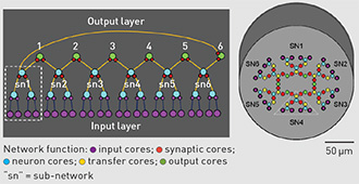
Logical (left) and physical (right) layout of Cognifiber scheme. [Adapted from E. Cohen et al., Sci. Rep. 6, 29080 (2016); CC-BY 4.0]
Bhaskaran, Sebastian, Pernice and colleagues initially demonstrated photonic in-memory computation in 2018 using a single integrated optical device. Two years later, they carried out 64 matrix multiplications simultaneously by using directional couplers to divert the multiplexed output from an on-chip optical frequency comb to individual patches of PCM (the weights of the neural network). Given the potential speed of photonic modulation, the researchers say this “tensor core” could potentially carry out 2 trillion operations per second.
According to Bhaskaran, the work could result in a first prototype tensor core by the end of 2023 and then a commercial device a couple of years later. But he says it remains to be seen whether the “phenomenal performance” of their small device can be maintained at larger scales. And they still need to demonstrate exactly how their processor interfaces with the electronics that sets its weights, given the differing scales of the two technologies—light having wavelengths of hundreds of nanometers, while transistors in microchips tend to be just a few tens of nanometers long. “That is a huge research question that we are addressing,” he says.
The connection problem
This thorny problem of linking photonics to electronics is one faced by almost all developers of photonic computers. One company taking a novel route to address it is Israel-based Cognifiber. Its scheme abandons silicon photonics altogether and instead turns to glass, in the form of multicore optical fibers. The idea is to exploit interference between cores to mimic interactions among neurons and synapses in a multilayer neural network (see “Mental fiber,” right).
Given the difficulty of linking photonic processors to the electronic world, some companies have decided that it’s best not to try. That is the approach taken by California-based Ayar Labs, which was founded in 2015 to commercialize optical interconnects. The company’s co-founder and CTO Mark Wade says that he and his colleagues sat down and concluded that the speed-limiting, energy-sapping movement of data between processors was likely to prove a bigger bottleneck than the performance of the processors themselves.
Wade says that with some US$195 million in funding and around 100 staff on its books, Ayar Labs is now preparing two optical I/O products for mass production: an optical “chiplet” that converts electrical signals to and from optical pulses at speeds of up to one terabyte per second, and a fiber-connected laser to provide the light. The idea is to connect components over tens of centimeters or more—across a given board, between boards on the same rack or between racks—rather than enhancing communications within monolithic chips.
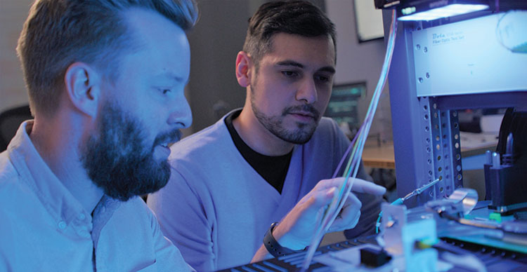 Ayar Labs CTO and co-founder Mark Wade (left) and an engineer inspect the company’s SuperNova multiwavelength laser sources in the lab. [Ayar Labs]
Just talk?
Expecting to reach full production by the end of 2026, Wade is confident that Ayar Labs has made the right choice in not pursuing photonic processing. And he adds that his company is not alone, noting that other businesses set up to develop photonic computers “are starting to pivot towards optical I/O.”
Indeed, another California outfit called Luminous Computing has changed tack. The company declined to provide any details to OPN, but its online marketing literature states that around three years ago it switched focus from photonic computation to chip-to-chip communication. Its aim now is to build “the world’s most powerful, scalable AI supercomputer” by using photonics to link up electronic chips in what it claims is a completely novel system architecture. The firm says it has raised around US$125 million to date, assembled a team of 100 people and is currently looking to hire another 100.
Likewise, Hamerly, now working at NTT Research in Sunnyvale, CA, USA, reckons there are “good reasons to be skeptical” about optical computing, even if it could potentially bring greater benefits than optical interconnects. He argues that while there are fundamental limits to the scaling of electronic computation related to quantum tunneling, the restrictions on the minimum size of optical components—such as the wavelength of light used and the bending radii of ring resonators or waveguides—are still more severe. “You’re never going to get the same density of components with optics as with electronics,” he says.
Harish Bhaskaran foresees photonics and analog electronics being used together on the same chip to maximize throughput while enabling scaling.
In fact, both Lightmatter and Lightelligence have released optical-interconnect products in addition to their processors. Harris says that although he and his colleagues founded Lightmatter to develop photonic processors, they realized that they “would hit a wall” in not being able to feed data to the chip quickly enough; hence the development of their interconnect. But he maintains that photonic computation is well worth pursuing, describing it as “a much harder problem but with much higher impact” than that of communication.
Bhaskaran is also confident, but cautious. He foresees photonics and analog electronics being used together on the same chip to maximize throughput while enabling scaling. But he says it is not yet clear whether applications exist for which such chips would offer an unambiguous advantage over digital electronics—and, therefore, whether they really will be a commercial success. “That remains to be seen,” he says.
Edwin Cartlidge is a freelance science writer based in Rome, Italy.
References and Resources
-
Y. Shen et al. “Deep learning with coherent nanophotonic circuits,” Nat. Photon. 11, 441 (2017).
-
E. Cohen et al. “Neural networks within multi-core optic fibers,” Sci. Rep. 6, 29080 (2016).
-
R. Hamerly et al. “Large-scale optical neural networks based on photoelectric multiplication,” Phys. Rev. X 9, 021032 (2019).
-
J. Feldmann et al. “All-optical spiking neurosynaptic networks with self-learning capabilities,” Nature 569, 208 (2019).
-
J. Feldmann et al. “Parallel convolutional processing using an integrated photonic tensor core,” Nature 589, 52 (2021).
