

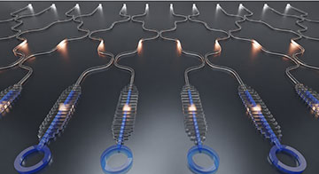
Artist’s impression showing how diamond nanobeams (blue) are meshed with a titanium dioxide integrated circuit using fishbone-shaped photonic crystal cavities. [Image: Shuo Sun et al.]
Scientists in the United States and the Republic of Korea have shown how to overcome the tricky problem of combining materials able to efficiently emit quantum particles with those best suited to making integrated quantum circuits (Light: Sci. Appl., doi: 10.1038/s41377-026-02339-w). They reckon that their scheme, which exploits self-alignment to minimize coupling losses between diamond and titanium dioxide, should make it easier to scale up quantum computers and networks.
Scaling fabrication
Physicists can now routinely generate single and entangled photons from a range of solid-state systems, including semiconductor quantum dots, diamond color centers and organic molecules. However, fabricating photonic circuits at scale in such materials remains an ongoing challenge. On the other hand, the materials that lend themselves naturally to such fabrication—such as silicon, silicon nitride and lithium niobate—cannot be made to efficiently emit photons with the desired line widths and coherence times.
One way to get around these problems is to realize heterogeneous integration: combining two different materials on the same platform. This strategy has proved a success in classical photonics, permitting, for example, the combination of lasers made from III-V semiconductors and low-loss materials such as silicon. However, quantum circuits are more demanding. Even a slight mismatch in coupling across the interface of the materials can destroy the delicate states of nonclassical light.
Leveraging heterogenous integration
In the latest work, a group headed by Shuo Sun at JILA and the University of Colorado Boulder, USA, has shown how heterogeneous integration could be applied to quantum circuits. The team did so by patterning a resist with the shape of a fishbone photonic‒crystal cavity and inserting a 200-nm-wide diamond nanobeam into the pattern’s spine. After depositing a layer of titanium dioxide (which is well suited to integrated photonics) across the resist and then removing the latter, the researchers were left with a titanium dioxide cavity that coupled almost seamlessly to a silicon vacancy center in the diamond.
Key to the process, they say, was the insertion of the nanobeam made from electronic-grade single-crystal diamond. They point out that both the beam and fishbone cavity spine are narrower than the wavelength of visible light, making it impossible to guide the operation using an optical microscope. So they shaped the end of the spine into a funnel, allowing the cavity itself to guide the nanobeam (held with a tungsten probe) into place—the funnel correcting the orientation of the beam in a series of steps until it lined up with the spine.
They established the scattering loss at the interface between the titanium dioxide and diamond to be no more than 1.3% at a wavelength of 737 nm. They then carried out a number of tests to demonstrate the performance of their setup, showing that the cavity at least quadrupled the vacancy center’s emission rate. They also established control over the emitted photons’ spin and read out the spin using the titanium dioxide photonic chip.
Toward more complex devices
What’s more, they showed that inverse design should make it possible to build more complex devices. In particular, they simulated the construction of a quantum light extractor that directs broadband emission from a color center into a single mode within a waveguide—an essential component, they say, for chip-integrated single-photon sources.
“Together, these results represent a significant step toward scalable, high-efficiency integration of solid-state quantum emitters with large-scale photonic circuits,” they write, adding that their scheme is not limited to diamond and titanium dioxide but could be applied to “a wide range of solid-state quantum emitters integrated with thin-film photonic devices where conformal deposition is feasible.”
The researchers point out that the technique they currently use for depositing the titanium dioxide—atomic layer deposition—is slow and not well suited to producing photonic circuits several hundred nanometers thick. But they say that their devices could be made using quicker methods, such as physical vapor deposition, so long as they can ensure that all surfaces in an integrated circuit are coated uniformly.
They also note that the maximum Q value they achieved in their experiment, 4,600, is not exceptional. But here too they argue it should be possible to make significant improvements because they are currently limited by loss within the titanium dioxide and fabrication imperfections rather than through the integration of the two materials. They say they should be able to push Q up to about 20,000, boosting emission rates by a further factor of 150, by optimizing lithographic exposure doses and stabilizing electron beam writing. Indeed, given suitably precise nanofabrication, the team believes it might be possible to approach Q’s theoretical limit of 100,000.
If the scientists can push their technology to these kind of performance levels, they claim it could be used to build a range of devices for quantum communication and information processing. In particular, by also integrating many emitters in large-scale circuits, they say it should be possible to build quantum repeaters featuring multiplexed memories, perhaps enabling quantum entanglement over national or even continental scales.
