

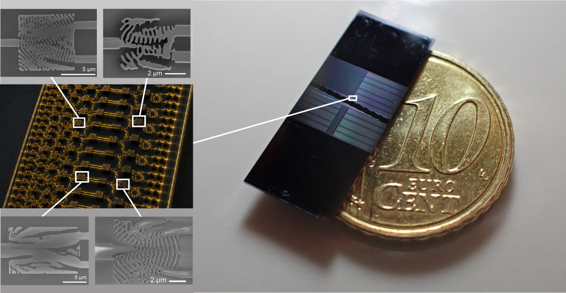
A photonic microchip next to a 10-euro-cent coin for scale. [Image: Tobi Bi / MPL]
Over the last decade, photonic inverse design has emerged as a powerful tool for solving complex problems that defy human intuition and standard building blocks. Unlike traditional approaches to photonic design, inverse design begins with desired device performance specifications and systematically generates a geometry that meets those targets.
Now, scientists based in Germany, the United States and China have leveraged inverse design to create photonic components on a silicon nitride platform that are up to 500 times smaller than conventional designs (Nat. Commun., doi: 10.1038/s41467-026-73390-9). The miniaturized components can be readily integrated into nonlinear and quantum photonic circuits, paving the way for scalable, high-performance silicon nitride‒based photonic systems.
Flipping design on its head
In forward design, researchers compute the optical response of a device starting from its geometrical description by means of a numerical simulation or a model. However, modern devices aim to exploit far more complex geometries with a large number of design parameters, rendering manual, intuition-based approaches insufficient. Inverse design methods can realize such complex device geometries and enable the development of improved photonic integrated components.
In the current study, the researchers applied iterative, gradient-based optimization to design, fabricate and test three types of inverse-designed devices: a wavelength-division multiplexer (WDM), mode-division multiplexer (MDM) and a reflector. While most inverse-designed structures have been implemented on the standard silicon photonic platform, they instead used a low-loss, foundry-compatible 800-nm-thick silicon nitride layer.
“Thick silicon nitride underpins most of the high-performance integrated photonics we work with, but until now its component library was limited to hand-engineered designs,” said study author Pascal Del’Haye, Max Planck Institute for the Science of Light, Germany, in a press release accompanying the work. “These compact, computer-designed components are an important step towards more densely integrated nonlinear and quantum photonic circuits.”
Footprint reductions
Del’Haye and his colleagues compared the size of their devices with more conventional silicon nitride implementations based on directional couplers or multi-mode interference couplers. The inverse-designed WDMs and MDMs ranged from 5 × 5 μm2 to 8 × 8 μm2 and 8 × 8 μm2 to 15 × 10 μm2 in size, respectively, corresponding to footprint reductions on the order of roughly 50 to 300 times for the WDMs and 500 times for the MDMs.
Lastly, the inverse-designed reflectors were used to construct Fabry-Pérot resonators with a 11 × 2.8 μm2 footprint and exhibiting a finesse exceeding 160 for a free space range of around 144.6 GHz and 307.6 GHz. In future work, the researchers plan to combine the new components with nonlinear optical circuits to generate optical frequency combs for applications in precision measurement, telecommunications and quantum technologies.
“Inverse design becomes practical when fabrication realities are built into the optimization,” said study author Kiyoul Yang of the Harvard John A. Paulson School of Engineering and Applied Sciences, USA. “By including minimum feature sizes and robustness to manufacturing variations in the algorithm itself, we obtain designs that are not only compact but also compatible with a commercial foundry process.”
