
![]()
Lindell Williams (left) and Grant Brodnik align an optical fiber with the edge of an integrated photonics chip. Optical fibers act as pipes for light, enabling the light generated on these chips to be collected and routed off the chip for use in experiments and applications. [Image: R. Jacobson/NIST]
Integrated photonics has the power to advance technology in areas such as telecommunications, visible-light consumer electronics and quantum computing. However, a well-known dilemma in the field is the fact that no single material is able to fulfill the diverse functional demands needed to build complex photonic systems.
“For example, some materials are good at making light directly, others are good at converting existing light to other colors or for realizing things like frequency combs,” said Grant Brodnik of the National Institute of Standards and Technology (NIST), USA. “Some are great for high-speed routing and switching but maybe only work well in the near-infrared and can’t operate across visible wavelengths.”
Now, researchers at NIST have developed a novel approach to heterogeneous integration for creating photonic chips that deposits patterns of specialized materials onto silicon wafers (Nature, doi: 10.1038/s41586-026-10379-w). The resulting chips combined lithium niobate and tantalum pentoxide, leveraging each material’s independent strengths on a single platform.
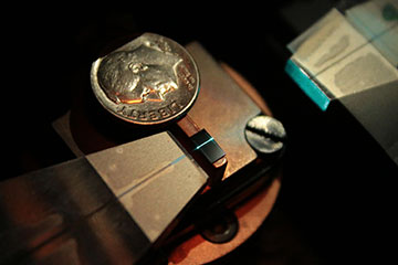
This small rectangular chip has been fabricated with numerous circuits designed to change the color of laser light. (A dime provides a size comparison.) [Image: R. Jacobson/NIST]
A unique ingredient
A key advantage of their method arises from the use of tantalum pentoxide, also known as tantala, a strong nonlinear photonic material suited to operating at visible wavelengths. Tantala has unique properties that make it well-suited for heterogenous integration, including room-temperature deposition, moderate-temperature annealing and low residual stress in thick films optimized for phase matching.
“[Tantala is] differentiated by its ability to be fabricated using processes that maintain compatibility with other photonic platforms,” Brodnik said. “Things like low-temperature processing steps and deposition of tantala—we can essentially ‘sprinkle’ the material directly on top of other materials—mean we can put tantala directly onto existing photonic circuitry, allowing different materials with different strengths to operate in concert.”
In the end, Brodnik and his colleagues were able to achieve monolithic 3D integration of tantala integrated photonics directly on a thin-film lithium niobate photonic substrate. By patterning the two materials on top of each other in a 3D stack, their technique allows for seamless integration and incorporation of nonlinear optics directly into existing and emerging photonics infrastructure.
A rainbow of colors
As a demonstration of their method, the researchers combined the capabilities of upper-layer tantala (four-wave-mixing optical parametric oscillation) and lower-layer lithium niobate (second-harmonic generation) to unlock arbitrary-wavelength laser conversion. They fit roughly 50 fingernail-sized chips containing 10,000 photonic circuits, each outputting a unique color, onto a single wafer.
“Applications that access atomic transitions need optical sources spanning the visible and near-infrared wavebands,” said Brodnik. “Current laser technology limits their use to larger scale laboratory environments. Making compact sources could unlock field deployable systems.”
