
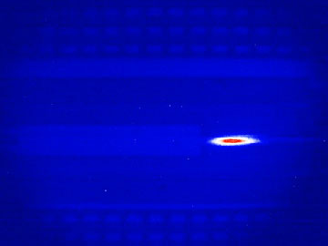
A snapshot of light's evolution within the multimode interferometric device. [Image: Technion Spokesperson Office]
With integrated photonic circuits finding use in an ever-greater range of applications, their complexity is on the rise. This increases the chance of minuscule defects creeping in during fabrication, but scientists have yet to find a fully satisfactory way of characterizing chips’ performance.
Now, researchers in Israel have shown how to exploit the natural nonlinearity of silicon to track the propagation of light through a circuit (Optica, doi: 10.1364/OPTICA.504397). They say that their technique, which they demonstrated in integrated waveguides and beam splitters, is simple to implement and completely noninvasive.
Limited quality control
Integrated photonics exploits the manufacturing infrastructure of modern electronics to fabricate photonic circuits precisely and cheaply using high-resolution lithography. These circuits combine a variety of miniaturized optical components, such as waveguides, resonators and beam splitters, which are arranged to form devices that can be used in data centers, laser ranging, matrix multipliers for machine learning and even quantum computers.
Given the difficulty of identifying all of the defects that accumulate during the manufacturing process, photonic chip developers need to accurately measure how light flows through these circuits. A number of such characterization techniques already exist, but all have their limitations. Far-field scattering, for example, tends to degrade the signal that is being monitored, while near-field microscopy involves impractically long scanning times and can be blocked by the protective layer that often covers such circuits.
In the latest work, Guy Bartal and colleagues at the Technion-Israel Institute of Technology in Haifa claim they can overcome these limitations by utilizing the nonlinear process of four-wave mixing. The idea is to irradiate an integrated circuit with a pump laser from directly overhead so that two photons from the pump interact with a signal photon propagating along the device. This process yields a fourth photon that travels away from the circuit―making it detectable―and whose electric field encodes that of the signal photon.
Characterizing light propagation
The researchers demonstrated their technique by splitting the output from a femtosecond infrared titanium–sapphire laser and doubling the wavelength of one half to create a telecom signal pulse. At the same time as coupling that pulse to a silicon-on-insulator waveguide (from a pre-existing biomedical imaging circuit) they routed the other half―the probe pulse―along a delay line and through a focusing lens so as to meet the signal pulse on the circuit. They then passed the nonlinear output pulse the other way through the lens, separated it from the pump pulses using a dichroic mirror and imaged it with a standard CMOS camera.
In doing so, they mapped the electric field distribution of the signal pulse in the waveguide and compared that with the results of a computer simulation―finding excellent agreement between the two for pump pulses polarized both parallel and perpendicular to the signal propagation direction. By adding a single lens to their setup, they also recorded images in the spatial-frequency (Fourier) domain—and used the image they acquired to calculate the signal's phase velocity through the waveguide to be about 1.3 × 10⁸ m/s.
Then, to characterize light propagation in more complex devices, they directed the signal and pump pulses at a "multimode interferometric" beam splitter. Such a splitter works by taking light from a single waveguide, diffracting it in a broader piece of silicon and constructively interfering different parts of the wavefront so that the peaks overlap with two narrower output waveguides. Directing the probe pulse at the signal pulse as it traversed successive portions of the beam splitter, the researchers were able to image the evolution of the interference process, again in good agreement with the simulation.
Cheaper and simpler
Bartal and colleagues say that because their technique is based on the nonlinearity of silicon and other semiconductors, it does not change photonic devices in any way that could impair their performance.
Bartal and colleagues say that because their technique is based on the nonlinearity of silicon and other semiconductors, it does not change photonic devices in any way that could impair their performance. Specifically, it does not need coupling gratings or diffusers to be added during the characterization process, nor does it require protective oxide layers to be removed from the surface of the devices. As such, they claim that their method “has the potential to drastically decrease the cost and complexity of integrated photonic circuit characterization, while increasing their availability.”
To this end, the researchers would like to expand the technique's field of view in order to map the light throughout a whole wafer in a single shot. But they point out that doing so would require a much more powerful laser for the probe―so as to maintain a decent energy density as the beam expands―as well as a custom-made objective lens. A more practical solution, they say, would be to use a motorized stage capable of reaching every point in the wafer and characterizing it via a moderate field of view.
