
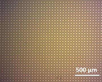
Researchers developed a continuous roller printing process that can pick up and transfer more than 75,000 micrometer-scale semiconductor devices in a single roll with very high accuracy. An optical microscopy image of the roller transfer printing results is shown. [Image: E. Margariti, University of Strathclyde]
Most people have had the experience of rolling out cookie dough or sheets of clay. A high-throughput manufacturing process, roller transfer printing, could bring similar ease and efficiency to creating arrays of tens of thousands of micro-LEDs (Opt. Mater. Express, doi: 10.1364/OME.483657).
In the new technique, scientists carefully transfer the tiny semiconductors from their growth substrate to a polymer film on a cylindrical roller. The method keeps the more than 75,000 individual pixels aligned with less than 1 μm deviation from their intended positions.
Harnessing adhesion
Micro-LED wafers, generally between 1 and 100 μm in size, make great high-contrast displays for many display devices, but they won’t work well unless they are aligned properly. Many of the pick-and-place schemes for assembling large-scale arrays of these semiconductor pixels rely on electrostatic or electromagnetic forces, or even thermomechanical responses driven by lasers. Pick-and-place might work for a handcrafted mosaic tile, but it would not be fast enough for commercial processes.
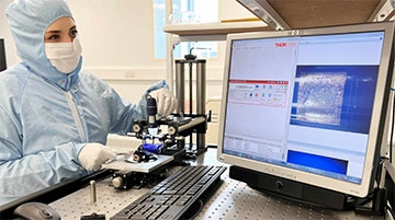
Eleni Margariti, who developed the new roller printing method with her colleagues, is pictured with the clean-room setup used to demonstrate the technique for rapidly manufacturing micro-LEDs. [Image: E. Margariti, University of Strathclyde]
Instead, Eleni Margariti and her colleagues at the University of Strathclyde, UK, eliminated the need to manage externally driven forces by harnessing the adhesion energy between a silicone roller and the deposition target. The roller, in the proof-of-concept experiments, was a commercially available silicone polymer cylinder 60 × 40 mm in size. Moving at constant velocity (8 mm/s) across the donor array, the roller grabs the III-N semiconductor pixels off their original silicon substrate, then deposits them on the recipient chip. The whole process takes about 20 s.
The Strathclyde team also developed an automated method for scanning the newly printed semiconductor array for defects. More than 99% of the pixels made it through the transfer process with a mean pitch error of 430 nm and a standard deviation of 980 nm.
Applications and goals
“This printing process could also be used for other types of devices,” said Margariti in a press release, “including silicon and printed electronics such as transistors, sensors and antennas for flexible and wearable electronics, smart packaging and radio-frequency identification tags.”
According to the researchers, the roller can be reused over and over with just a bit of cleaning in between runs. The team’s next goal is to increase the number of micro-LEDs that can be transferred with one roll. The researchers also say they want to combine different types of tiny chips onto the same substrate, and determine if it can be used to print to specific locations of the receiving platform.
