
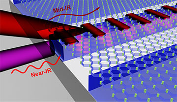
Researchers have devised a hybrid, hyperbolic–silicon photonic waveguide platform that transmits mid-IR and near-IR light at the same time, on the same chip, demonstrating dual-band optical processing. [Image: Caldwell Lab, Vanderbilt University]
As silicon waveguides carry more and more data through photonic chips, scientists have wished they could increase the bandwidth of the optical signals passing through these miniaturized platforms. Multiplexing near- and mid-infrared signals within the same waveguide, however, has challenged efforts to build chip-scale devices.
Now, researchers at a U.S. university have demonstrated a new hybrid waveguide that can carry mid-infrared (mid-IR, 6.5 μm to 7.0 μm) and near-infrared (near-IR, 1.55 μm) wavelengths simultaneously (Adv. Mater., doi: 10.1002/adma202004305). The waveguide, made of two different semiconductors, could form a key component of future integrated photonic structures that could handle data for telecommunications and chemical spectroscopy.
Stacking the components
The hybrid waveguide built at Vanderbilt University, USA, consists of a heterostructure of hexagonal boron nitride (hBN) and silicon. A heterostructure is “simply a stack of two different materials that share a common interface,” says Joshua D. Caldwell, an engineering professor at Vanderbilt. In this case, the materials are silicon and boron nitride—the latter in its most stable form, a hexagonal crystal lattice analogous to graphite.
Scientists already know how to make silicon waveguides to carry near-IR frequencies, but when they try to make mid-IR waves travel through the same material, they need to make the waveguide bigger. The problem is that a silicon waveguide large enough for mid-IR signals will mess up the near-IR transmission.
Enter hBN, which transmits the mid-IR waves as hyperbolic phonon polaritons. First by mathematical modeling and then by experimental work, the Vanderbilt team demonstrated that the researchers could form the hybrid arrangement by first etching waveguides into a slab of silicon some 220 nm thick, then transferring a 40-nm-thick layer of hBN on top of it. Scanning near-field optical microscopy allowed the team to analyze the modes of the signals passing through the heterostructure.
Future possibilities
Caldwell says that the heterostructure has many potential uses. “One is to use the mid-IR channel for chemical sensing, which could ‘inform’ the near-IR channel that a detection event occurred that could be used to route the signal to where it could be read out,” he explains. “Also, modulation of the mid-IR channel could be used to modify the local environment of the underlying silicon channel, thereby providing a means of actively modulating the near-IR signal. Finally, they could simply be used to transmit two different pieces of information in the same form factor.”
Next, Caldwell says he and his colleagues will investigate the integration of these hybrid heterostructures into functional silicon photonic structures, such as ring resonators and photonic crystals, to see if they can demonstrate near- and mid-IR multiplexing as well.
Researchers from three other U.S. institutions—the University of Iowa, Columbia University and Kansas State University—participated in the study.