
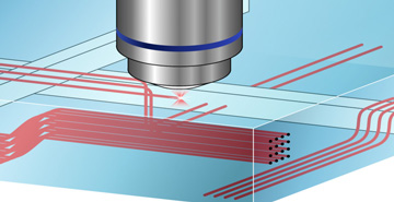
Researchers use multiphoton laser direct writing to create thin waveguides in silicone that could be used to transport light in a variety of sensors. [Image: Ye Pu / École Polytechnique Fédérale de Lausanne, Switzerland]
A team of researchers from the École Polytechnique Fédérale de Lausanne (EPFL) in Switzerland has demonstrated a new technique for fabricating compact, low-loss optical waveguides in a polydimethylsiloxane (PDMS) slab (Opt. Mater. Express, doi: 10.1364/OME.9.000128).
The method uses a femtosecond writing laser to initiate two-photon absorption in light-reactive monomers embedded in the PDMS. Two-photon absorption creates enough energy in the monomer molecules to trigger a chain polymerization reaction without the use of potentially toxic photoinitiator compounds. The resulting polymerized waveguides have a higher refractive index (RI) than the surrounding PDMS, making them efficient at confining light, and have a simpler chemical structure than photoinitiator-fabricated waveguides, making them potentially useful in biomedical applications.
Photoinitiator-free waveguides in PDMS
The EPFL team used a host–guest system and optimized multiphoton laser direct writing to fabricate its optical waveguides. The researchers chose PDMS as the “host” because the elastomer is transparent over a wide spectral range and has outstanding chemical and thermal stability. They chose phenylacetylene as the “guest” because it is a light-reactive monomer that is soluble in PDMS, can be polymerized without the help of a photoinitiator and has a high RI after it is polymerized.
To integrate the guest into the host, the researchers submerged the PDMS slab in a solution containing phenylacetylene for 24 hours. To carve out the waveguides, they used a femtosecond 60 mW Ti:Sapphire laser tuned to 680 nm to initiate the polymerization reaction of the phenylacetylene in the PDMS slab through two-photon absorption. A dichroitic mirror was used to guide the laser beam along the desired 3-D waveguide design.
Two-photon absorption generates enough energy in the phenylacetylene monomer molecules to initiate photopolymerization without needing an energy boost from photoinitiators. Photoinitiators increase light-absorption efficiency in light-reactive monomers, but they also increase the chemical complexity of the resulting waveguide and can, in some cases, be toxic, prohibiting their use in vivo.
Polymerized phenylacetylene has a higher RI than PDMS, making it more effective at confining light within the waveguide. In demonstrations, the researchers observed that their 1.3-µm-thick optical waveguide exhibits only a 0.07 percent loss of transmitted light per centimeter for the 650 nm to 700 nm spectral band.
Next steps: Optimization and application
The EPFL colleagues hope to improve their fabrication process by optimizing the control system that reduces material damage during laser writing. With an optimized setup, they say that they could create waveguides less than 1 µm thick.
They are currently working on a flexible endoscope design that is less than 1 mm in diameter and contains an array of their waveguides in PDMS. Team member Ye Pu said in an OSA press release that “such a small, mechanically flexible endoscope would allow a number of hard-to-reach places in the body to be imaged for diagnosis in the clinic, or for monitoring in a minimally invasive surgery.”
Other potential applications for the waveguides include biosensors, microfluidic flow cytometry, electro-elastic optical modulators, flexible optical circuit boards, wearable and implantable photonic devices and optical neuron stimulation.
