
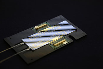
Bristol-NTT device reportedly offers a chip-scale laboratory for quantum optics. [Image: University of Bristol]
Scientists in the United Kingdom and Japan have fabricated a glass chip with an optical waveguide circuit that’s capable of implementing a universal set of linear optical transformations—and that can be reprogrammed on the fly (Science, doi: 10.1126/science.aab3642). The researchers believe that the device, by making some key optical building blocks of quantum-computing protocols available in a flexible, reprogrammable platform, could dramatically reduce the time and resources required to fashion quantum-computing experiments. “Now anybody can run their own experiments with photons,” says team leader Anthony Laing of the University of Bristol, U.K., “much like they operate any other piece of software on a computer.”
Since Richard Feynman first proposed the idea in 1982, physicists have dreamed of a computer built on quantum-mechanical principles such as entanglement, and capable of simulating problems in domains (such as quantum physics itself) beyond the reach of classical computers. But, although vast progress has been made in pieces of the problem—developing quantum algorithms, fashioning optical quantum logic gates, preparing and manipulating single photons—the creation of a flexible, programmable platform analogous to classical computers has proved a challenge. As a result, setting up and refining quantum-computing experiments can consume months of research time.
Goal: reprogrammable, universal linear optics
Liang’s team at Bristol, in partnership with researchers at the Nippon Telegraph and Telephone Corporation (NTT) in Japan, attempts to address part of that problem in the new device. The scientists focus in particular on linear optical (LO) circuits, which they say “lie at the heart” of quantum information protocols and of implementing core processing functions on optical qubits. The Bristol-NTT group set out to design a chip that was “completely reprogrammable and universal” for linear optics, and that thus could provide a flexible platform for testing quantum technologies.
The device they built consists of a silica-based planar waveguide circuit etched onto a silicon wafer; the germanium-doped silica waveguide core has a cross-sectional dimension of 3.5 μm square. The circuit includes 15 Mach-Zehnder interferometers (MZIs), across six optical modes, fashioned from 30 tunable phase shifters and beam splitters.
The scientists then tied an 808-nm pulsed Ti:sapphire laser to the device, passing the light through barium borate nonlinear crystals to create paired photons that were shunted into the chip through optical fiber. A separate electrical circuit allowed arbitrary control of the on-chip MZI systems, to quickly reprogram the chip through different LO circuit networks; a given LO network on the chip corresponded to a specific set of phase values read at the end of the line.
“A year’s worth of experiments in a matter of hours”
With this setup, the team was able to configure the chip across more than 100 different settings, and to demonstrate a variety of standard quantum information processing protocols, including an entangling quantum gate, quantum process tomography and boson sampling. More to the point, they were able to reprogram the chip on a timescale of seconds to milliseconds. “We carried out a year’s worth of experiments in a matter of hours,” says Ph.D. student Jacques Carolan, the first author on the study.
While the device provides “universal linear optics” only for a system of six optical modes, it appears to constitute an important proof of principle for reconfigurable optical circuits, an essential technical building block for quantum information processing. The Bristol-NTT team expects to push its work forward with additional chips and make them available to the research community through Bristol’s “Quantum in the Cloud” program.