
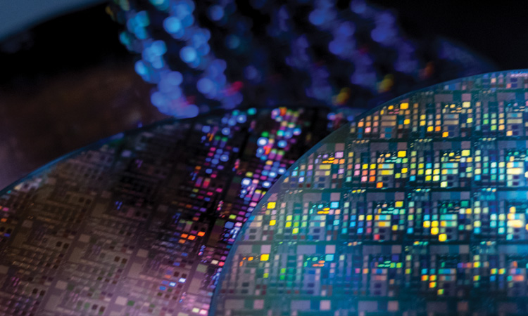
 [N. Cooper / Getty Images]
As semiconductor features approach atomic dimensions, the industry’s most advanced production tools—the ASML NXE & EXE extreme ultraviolet (EUV) lithography scanners—are running out of photons. Free-electron lasers (FELs), which use relativistic electron beams to generate light millions of times brighter than conventional lasers, promise four times the power at half the energy cost. This article explores how FELs work and how they could not only address today’s lithography bottlenecks, but also provide a clear path toward sub-nanometer nodes.
Chasing Moore’s Law to the atomic scale
Imagine trying to write your name with a pencil the size of a telephone pole. That is the precision challenge facing modern semiconductor manufacturing, driven by the relentless demands of Moore’s Law.
In 1965, Gordon Moore observed that transistor density doubles roughly every two years—a prediction that shaped the trajectory of the semiconductor industry for decades, as both benchmark and self-fulfilling prophecy. From just a thousand transistors per chip in 1970, we’ve reached over 100 billion today, and some experimental devices have demonstrated more than one trillion.
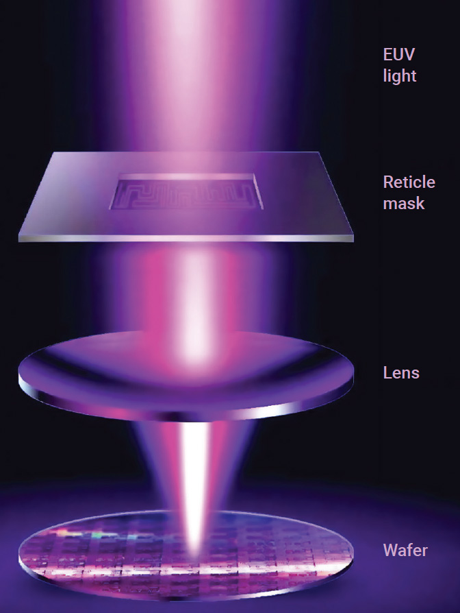 [Enlarge image]Illustration of the EUV lithography process for semiconductor manufacturing. [xLight]
Sustaining this pace requires extraordinary technological leaps, none more ambitious than EUV lithography, which operates at a wavelength of 13.5 nm (10 times shorter than previous deep UV technology) and is the key to achieving near-atomic-scale features.
Operating at these extreme wavelengths introduces formidable challenges: Virtually all materials, including air, strongly absorb EUV photons. This makes EUV equipment expensive and difficult to produce. Special EUV lithography masks are used, featuring multilayer stacks of molybdenum-silicon reflectors, capped with a thin ruthenium layer. These ASML scanners cost more than US$200 million each (twice as much for the newer models) and require mirror polishing precise to within a single atom. Mark Phillips, Intel’s director of lithography hardware, calls the EUV scanner “the most technically advanced tool of any kind ever made,” and that’s barely hyperbole. But while building the machine is a significant challenge, powering it with enough light is equally difficult.
Today’s sources: laser-produced plasma
The current state-of-the-art EUV light source, laser-produced plasma (LPP), is truly a feat of engineering. A molten tin droplet is injected into a vacuum chamber 50,000 times per second. For each droplet, a carefully timed “pre-pulse” laser reshapes it into a disk shape, before a second, high-power CO2 laser pulse vaporizes it. This main pulse heats the tin to over 200,000°C—40 times hotter than the sun’s surface—triggering electron transitions that emit the desired 13.5 nm photons. This process has some drawbacks:
Power: Generating EUV photons via any process, and not just LPP, is notoriously inefficient. Generating 500 W of usable EUV output requires about 1 MW of input power (0.05% efficiency). Given that semiconductor fabs already consume significant portions of national power grids (TSMC alone accounts for roughly 10% of Taiwan’s energy consumption) the urgency for better EUV sources grows acute.
Heat and debris: Most of the energy in the LPP process is lost as heat and molten tin debris, which contaminates and heats up the collector mirror. To combat the contamination, 600 liters of hydrogen per minute are pumped into the source chamber to form a “hydrogen curtain.” Despite this, collector lifetime still represents a significant operational cost. The mirror heating further limits the output power of the LPP tool.
Precision: LPP is unpolarized and broadband. The ASML scanner “selects” the useful part of this light to expose the chip, leading to photon scarcity and stochastic failures—random variations in photon absorption and pattern fidelity due to low photon number—that degrade chip yields as transistor dimensions shrink.
The LPP source is an amazing tool, but as the push to scale EUV lithography demands more and more light, we need a different kind of physics.
The next rung on the brightness ladder
Fortunately, a promising alternative to LPP sources already exists: the FEL. While FELs can generate many times more EUV power at a fraction of the energy cost and with unmatched beam quality, their decisive advantage as a light source is a quality known as “brightness,” the crucial metric for lithography and beyond.
Brightness is a technical term that combines optical power P, quality of focus (area A, solid angle Ω), and spectral purity (relative bandwidth Δλ/λ):
B ~ P / (A × Ω × Δλ/λ)
This exceptional brightness stems from a fundamental distinction: the “free” versus “bound” electron nature of the light source.
 [Enlarge image]Comparative maximum brightness of light sources: The “ladder of brightness” plots the spectral radiance of light-source technologies on a logarithmic scale spanning 30 orders of magnitude. [D. Black]
Conventional “bound-electron” sources, from incandescent filaments to today’s LPP sources, are ultimately constrained by the properties of their materials, be it a melting temperature or the fixed atomic emissions of vaporized tin. FELs, by contrast, are “free-electron” sources that transcend this constraint. They have three unique advantages:
No damage limit: Free electrons in vacuum can’t be damaged by intense fields, unlike the solid-state gain media of conventional lasers.
Highly selective amplification: The FEL resonance condition, governed by special relativity, ensures only perfectly matched photons are amplified, giving extreme spectral purity.
Coherent emission: Electrons are “microbunched” into dense, sub-wavelength clusters that radiate in perfect unison, a coherent process that quadratically enhances the light’s power.
In an FEL, electrons travel freely in vacuum at almost the speed of light and exchange energy with a co-propagating electromagnetic wave, giving rise to an exponentially amplified tunable light beam.
Anatomy of an FEL
In an FEL, electrons travel freely in vacuum at almost the speed of light and exchange energy with a co-propagating electromagnetic wave, giving rise to an exponentially amplified tunable light beam.
High-energy electron beams: The process begins with a high-energy electron beam from a particle accelerator. Microwave amplifiers accelerate electrons to nearly the speed of light. For a 1 GeV beam (that’s one electron charge times 1 gigavolt), electrons are slower than light by only one part in 10 million. The more energetic the electron beam, the higher the photon energy the FEL can produce.
Wigglers versus undulators
Wigglers and undulators are distinguished by the K parameter, which is proportional to the magnetic field strength and the amplitude of the electron oscillations.
When K < 1: The oscillations are small, and the light is primarily emitted at a single frequency in the forward direction. The device is called an undulator.
When K > 1: The oscillations are large, the emission angle is wider and the light is broadband. The device is usually called a wiggler.
An FEL is typically operated with a small K parameter (thus an undulator). However, FEL output is orders of magnitude brighter than spontaneous undulator radiation because it is coherently amplified.
Accelerating charges radiate: Any accelerating charge radiates light. A bremsstrahlung (German for “braking radiation”) source slams electrons into a wall, rapidly decelerating them, and the beam sheds its energy as light and heat. A bending magnet works too. If you bend the beam in a circle, you have a synchrotron source. But if you wiggle it in a sine wave, you have a wiggler or an undulator.
Synchrotron and wiggler sources produce fairly broadband light, but the undulator is a different story. When operated under just the right conditions, an electron beam in an undulator can lase.
The undulator: An undulator is a periodic array of magnets that make a high-energy electron beam oscillate, or “wiggle,” in a sine wave with a specific frequency. This controlled oscillation of the electron bunch is the first step in producing precisely tuned light. The period of the undulator, λu, along with the beam energy, determines the output wavelength of the light.
 [Enlarge image]Schematic of an FEL. The inset shows the wiggling electron path producing light waves at the turnaround points. [Tristanevanslee / Wikimedia Commons; CC-BY-1.0]
Slippage and color selection: The FEL process exploits “slippage” to help select one color of light. In the undulator, electrons travel at near-light speed, but not quite. Since they’re also wiggling in a sine wave, they travel a slightly longer distance than the equivalent straight-line path. The light beam, of course, travels precisely that straight-line path at light speed, and thus wiggling electron beams in an undulator are very slightly outpaced by the light wave they create.
At the resonant wavelength condition, the electron bunch slips back relative to the light by exactly one (light) wavelength for each wiggle the electron bunch completes. This is a synchronicity condition that allows continuous amplification of the light by the electron beam, and from it we can derive the FEL radiation formula:
λr= λu / (2γ2 ) (1 + K2/2)
where λu is the undulator’s magnetic period, λr is the radiation wavelength, γ is the electron’s relativistic energy and K is a parameter describing the magnetic field strength.
Microbunching and coherent radiation: Since the electron beam contains many electrons, the strongest amplification occurs when the light emitted by each electron adds up in-phase, that is, coherently. This is the “laser” part of a free-electron laser. The light field created in the earlier steps acts back on the electrons, sorting them into dense, periodic clusters—microbunches—spaced exactly one wavelength apart.
To visualize the microbunching process, imagine an electron absorbing a photon: It gains a tiny amount of energy and travels a bit faster. Another electron ahead of it may radiate a photon, losing energy and slowing down. The faster electrons catch up to the slower ones, forming microbunches of densely packed electrons.
Since the electrons within a microbunch are nearly on top of each other, they all radiate coherently. But this light field acts back on the electron beam in a feedback loop, increasing the microbunch density and their energy spread, which causes even more amplification in an exponentially growing process. Eventually, the energy spread of the microbunches overwhelms the density compaction, and they begin to de-bunch. This stage is called saturation, beyond which amplification stops.
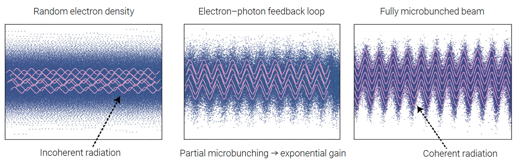 [Enlarge image]Microbunching and coherent radiation: The initial electron beam starts with no density modulation, so its radiation is incoherent (left). As electrons travel through the undulator, their interaction with the growing light field sorts them into microbunches (center). These microbunches, spaced exactly one wavelength apart, radiate in perfect unison, causing exponential amplification of the light, until the emission is fully coherent (right). [D. Black, D. Nguyen]
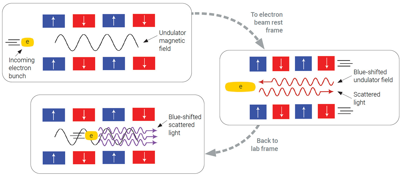
The relativistic factor enables high-energy light: One mystery remains about the FEL process: How does it produce such high-energy (small-wavelength) light, in this case EUV light with a tiny wavelength of 13.5 nm, when the undulator magnets have such a large period, a few centimeters? The answer lies in a double-boost of special relativity, sandwiched around a scattering event.
One mystery remains about the FEL process: How does it produce such high-energy (small-wavelength) light when the undulator magnets have such a large period, a few centimeters?
Consider the reference frame of the undulator magnet. In it, the undulator is stationary with period λu , and an electron beam flies toward it at nearly the speed of light. In the electron’s rest frame, the situation is reversed; the electron bunch is stationary, the undulator appears to fly toward it. Therefore, in the electron rest frame, the moving undulator appears Lorentz-contracted and its period shortens by a factor γ, becoming λu /γ. That’s one boost.
The undulator magnetic fields are transformed in the electron beam frame. To the stationary electrons, the moving undulator magnetic fields look just like incoming light waves. These waves scatter off the stationary electron bunch, sending radiation back in the opposite direction. That’s the scattering event.
The RLS tradeoff
For decades, photoresist performance has been constrained by the RLS tradeoff equation:
Blur3 × LER2 × Dose ~ constant
This means improving any one parameter (resolution, line-edge roughness (LER) or sensitivity) inevitably degrades the others. For example, traditional resists achieve high sensitivity through chemical amplification, but the amplifying acid diffuses randomly, creating blur. New metal oxide resists could eliminate acid diffusion entirely, potentially improving resolution and reducing roughness. Similarly, higher power FEL sources relax the dose requirement, allowing optimization for LER and Blur.
After the scattering, we leave the electron beam frame and transform back to the lab frame to observe the scattered light. In the lab frame, the detector sees the electrons rushing toward it at near light speed. But it also sees the scattered light wave, which is Doppler-shifted (blue-shifted) by an additional factor of ~1/ (2γ), resulting in a final wavelength proportional to λu /2γ2. The undulator fields are also transformed back to their original, stationary selves with period λu . That’s the second boost, completing the process.
Usually, γ is large, equal to 1000 or more for an EUV FEL, with an output wavelength millions of times shorter than the undulator’s physical period. This allows us to produce nanometer-scale wavelengths with only centimeter-scale magnets. Better yet, this makes the light source tunable, as only a small change in γ—electron beam energy—alters the outgoing light frequency.
 [Enlarge image]Centimeter-scale magnets produce nanometer-scale light through relativistic transformations. This “double relativistic boost” converts the centimeter-scale undulator period into nanometer-scale radiation. [D. Black]
From lab to fab: toward industrial EUV
These six steps give us a good understanding of how FELs work. But while the physics of an FEL is elegant, its true value lies in solving the specific, pressing challenges facing semiconductor manufacturing as we push toward atomic-scale features. The FEL isn’t merely a more powerful light source, it’s a fundamentally better-matched tool for the Angstrom era.
As transistor dimensions shrink, stochastic defects start to hurt the yield. There’s only one solution: more power. The FEL is the one technology with a demonstrated path to the multi-kilowatt regime.
Consider the immediate technical advantages. Next-generation high-numerical-aperture EUV scanners rely on steep ray angles that cause contrast loss when using unpolarized light from plasma sources. FELs, by contrast, naturally produce polarized light, maximizing pattern fidelity where it matters most. Their coherent, narrow-band output was once seen as a challenge due to speckle effects but is mitigated in the current scanner design by an ingenious multi-part illumination system. It is now understood as an opportunity, enabling new in-situ metrology techniques that are impossible with the chaotic light from plasma sources.
But the most compelling argument for FELs is their scalability. As transistor dimensions shrink, stochastic defects, which are random variations in pattern exposure due to photon scarcity, start to really hurt the yield. There’s only one solution: more power. The FEL is the only known technology with a demonstrated path to the multi-kilowatt regime.
Increasing efficiency: ERLs
A key technology that makes industrial FELs power efficient is the energy-recovery linac (ERL). After the electron beam passes through the undulator and creates light (losing only a tiny fraction of its energy), it is not discarded. Instead, it is looped back through the accelerator, but 180° out of phase with the accelerating field of the accelerator cavities. At the decelerating phase, the electron beam transfers most of its remaining energy back into the accelerator cavities, where the stored energy is then used to accelerate the next batch of fresh electrons. This recycling process improves the wall-plug efficiency of the entire system.
The economics tell an equally compelling story. An LPP source consumes 1.1 MW to generate 500 W of EUV light—8.8 MW draw to power eight EUV scanners. By contrast, an FEL facility can deliver 2000 W to each of eight high-NA scanners while consuming only 4 MW in total—four times the light at half the energy cost. Replacing pure niobium (Nb) superconducting cavities in the accelerator with Nb3Sn could reduce this still further to a 2 MW total power draw, making the FEL more than 16 times as power efficient as the current solution. Factor in the elimination of multi-million-dollar annual collector replacements, and a single FEL facility is not only technically superior but also cost-competitive, slashing operational expenses for the whole facility.
Perhaps most critically, the FEL wavelength is continuously tunable. Plasma sources are tied to specific atomic emission lines—tin atoms in the case of today’s LPP systems. When, or if, the industry moves to 6.7 nm, the tin plasma would have to be swapped out for another element. Gadolinium is the most likely contender, although its toxicity poses integration challenges. FELs avoid this by emitting a wavelength tunable by the electron beam energy, which offers a direct path to the shorter wavelengths for sub-nanometer nodes and beyond.
The light at the end of the tunnel
The transition to accelerator-based EUV sources represents more than an incremental improvement—it’s a paradigm shift as significant as the move from mercury lamps to excimer lasers a generation ago. By climbing to the pinnacle of the brightness ladder, FELs deliver not just more photons, but better photons: coherent, polarized, energy-efficient (at least relatively so) and precisely tuned to the right color. FEL light sources are the next milestone in the quest for maximum transistor density.
Chris Anderson, Dylan Black, Kevin Heidrich and Dinh Nguyen are at xLight Inc., USA.
References and Resources
- D. Nguyen and C. Mayes, “VUV and X-ray Free Electron Lasers.” U.S. Particle Accelerator School, course materials for University of California, Davis (July 2024).
- J. Boyd, “Is the future of Moore’s Law in a particle accelerator?” IEEE Spectrum, June 10, 2024.
- H.J. Levinson, “Challenges and limits to patterning using extreme ultraviolet lithography.” J. Micro/Nanopatterning Mater. Metrol. 24, 1 (2024).
- ZEISS SMT, “Light of the Future: How does EUV lithography work?” ZEISS Semiconductor Manufacturing Technology Magazine, Dec. 6, 2022.
