
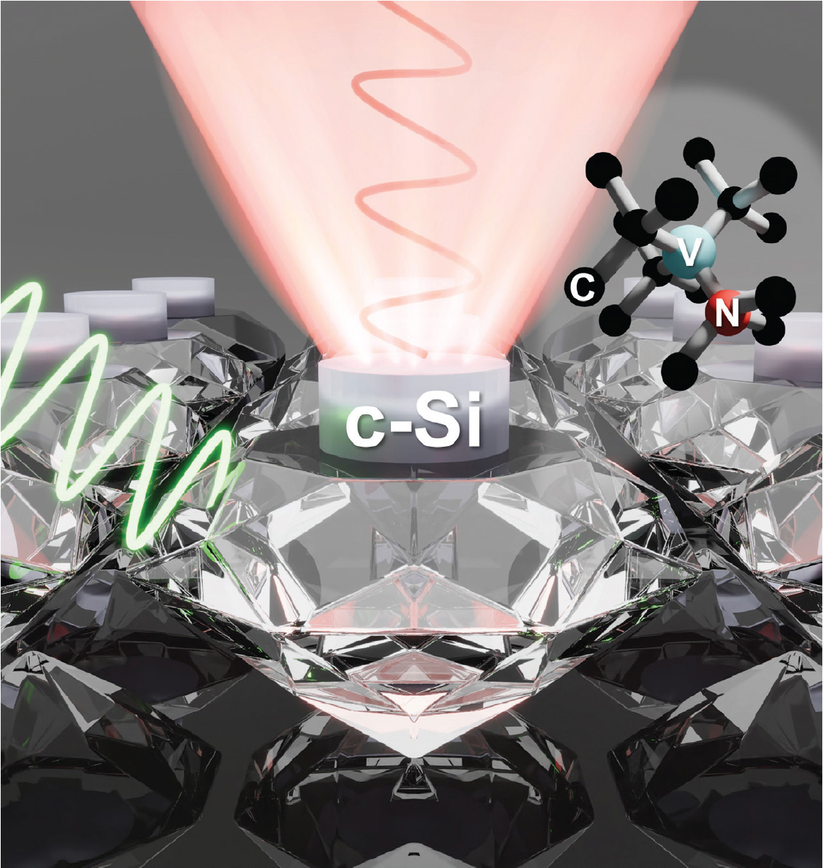
 [Enlarge image]Crystalline-silicon nano-antenna on diamond: 515-nm green pump excites a near-surface NV center; the red emission is beamed upward into free space.
Color centers in diamond, such as nitrogen-vacancy (NV) centers, have spin-dependent optical transitions that respond to external perturbations, making them effective sensors, especially of magnetic fields.1 Because of diamond’s high refractive index (~2.4), most photons emitted by NV centers are confined by total internal reflection and Fresnel reflections. Only 3–5% of NV-emitted photons reach free space, limiting optical readout.
Prior approaches, such as gratings2 or metasurfaces3 patterned directly into the diamond, can improve outcoupling but often degrade the quantum properties of near-surface emitters through surface roughening and altered surface chemistry.4 In a recent publication in Nano Letters, we addressed this outcoupling limitation with a surface-preserving, CMOS-compatible approach: a crystalline-silicon (c-Si) pillar on diamond that redirects NV emission into free space without etching the diamond.5
We chose c-Si for its high refractive index (~3.5) and modest loss across the NV emission spectrum (630–800 nm) due to its indirect bandgap, and because we were then able to use established Si microfabrication processes. The pillar fabrication starts with a common silicon-on-insulator (SOI) wafer, and the structure is designed to be rotationally symmetric to be compatible with all NV orientations. We optimized the structure using a spectrum-averaged figure of merit for broadband outcoupling with modest Purcell enhancement.
Using epitaxial lift-off methodology, we transferred a 220-nm c-Si membrane onto diamond implanted with 10-nm-deep NV centers, followed by e-beam lithography and Si etching. To protect near-surface emitters during processing, we intentionally left a thin Si layer (20–30 nm) over the diamond, maintaining surface quality while preserving NV properties. Under 515-nm excitation in a confocal microscope, we observed an increase of ~10× in collected count rate and a 2–3× reduction in NV lifetime, consistent with simulations.
Our c-Si antennas are scalable using standard foundry process flows and can be readily adapted to other diamond color centers, such as the silicon vacancy (SiV) and germanium vacancy (GeV) centers, as well as to quantum emitters in other wide-bandgap materials.
Researchers
M. Kim, J.T. Choy and M.A. Kats, University of Wisconsin-Madison, USA
References
1. S. Hong et al. MRS Bull. 38, 155 (2013).
2. J.T. Choy et al. Appl. Phys. Lett. 103, 161101 (2013).
3. T. Huang et al. Nat. Commun. 10, 2392 (2019).
4. S. Sangtawesin et al. Phys. Rev. X 9, 031052 (2019).
5. M. Kim et al. Nano Lett. 25, 4659 (2025).
