
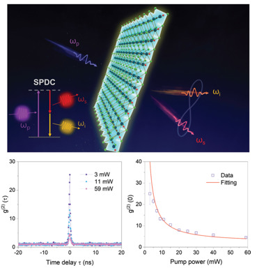
 [Enlarge image]Top: Artist's view of the SPDC process with a van der Waals crystal. Bottom left: Measured two-photon temporal correlation functions at different pump powers. Bottom right: Pump-power-dependent normalized correlation function at zero-time delay.
The generation of quantum entangled states is fundamental to optical quantum information processing, which involves coding, manipulation and detection of entangled photons. At present, the most versatile sources of entangled photons rely on spontaneous parametric down-conversion (SPDC) in χ(2) crystals, a nonlinear process in which a higher-energy pump photon is fissioned into a pair of lower-energy signal and idler photons.1
Almost all current entangled-photon sources using SPDC use conventional χ(2) crystals, such as BBO and LiNbO3 bulk crystals. The intrinsically low χ(2) coefficient of these conventional crystals, however, means a bulky size is necessary to ensure adequate SPDC efficiency. In work published this year, we used a novel 2D van der Waals (vdW) material to fashion an entangled-photon source less than 50 nm in thickness—to the best of our knowledge, the thinnest SPDC source ever recorded.2
As in classical photonics, chip-scale integration in quantum photonics has become crucial for scaling up and translating laboratory demonstrations to real-world technologies.3 Efforts in integrated quantum photonics center around the development of quantum photonic components capable of monolithic, hybrid or heterogeneous integration.4 A material platform with a high χ(2) coefficient and easy integrability is thus very desirable for constructing chip-scale SPDC sources—but such materials have proved elusive.
Recently emerging 2D vdW materials have shown exciting nonlinear properties; for example, their χ(2) coefficients are extremely high in monolayer transition metal dichalcogenides (TMDCs). However, their absolute χ(2) efficiencies are too low for practical nonlinear optical devices because of the vanishing light–matter interaction length at atomic thicknesses. Even worse, the χ(2) efficiency in such TMDC materials does not scale with thickness, because of issues related to structural symmetry and interlayer electronic coupling that degrade the χ(2) efficiency as thickness increases.
In our recent work,2 we discovered a novel vdW NbOCl2 crystal that shows both an unprecedented χ(2) coefficient and efficiency. The material has a giant χ(2) coefficient (comparable to that of monolayer TMDCs) regardless of thickness, due to noncentrosymmetry and vanishing interlayer electronic coupling; it also boasts a giant absolute efficiency, orders of magnitude higher than for TMDC monolayers. Given this vdW material’s scalable, giant χ(2) nonlinearity, we were able to use the material to construct an SPDC source as thin as ~46 nm for the first time.
We believe this work bridges the realms of quantum nonlinear optics and vdW materials—both extending the research boundary of vdW materials and opening a promising pathway toward urgently needed, chip-scale entangled sources for integrated quantum photonic circuits.5
Researchers
Qiangbing Guo, Cheng-Wei Qiu and Andrew T.S. Wee, National University of Singapore, Singapore
Xiaozhuo Qi and Xifeng Ren, University of Science and Technology of China, China
References
1. L. Li et al. Science 368, 1487 (2020).
2. Q. Guo et al. Nature 613, 53 (2023).
3. J. Wang et al. Nat. Photon. 14, 273 (2020).
4. E. Pelucchi et al. Nat. Rev. Phys. 4, 194 (2022).
5. J.L. O’Brien et al. Nat. Photon. 3, 687 (2009).
