
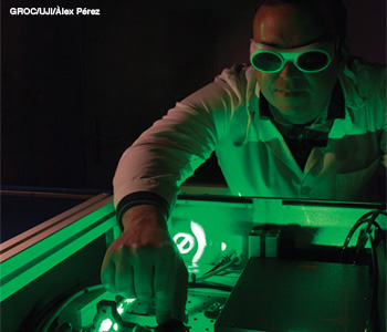
 An ultrafast laser delivers 27 fs optical pulses in the Photonics Laboratory, Universitat Jaume I, Spain.
Ultrashort-pulse lasers have been used for decades in industrial settings requiring powerful, precise processing of all kinds of materials. But innovation is hardly dead in this marketplace. In academic labs, advances in materials and laser configurations promise to open up a variety of new applications outside of the technology’s core area of industrial micromachining. And even within that core market, suppliers are pushing the envelope toward ever-shorter and more stable pulses, extending micromachining into previously untapped segments. Here’s an update on some recent developments on the ultrafast-laser scene.
The graphene difference
On the R&D front, particular interest currently centers on developing ultrafast lasers in the infrared, especially at around 2 µm. That’s a wavelength with broad potential applications—in telecom; in medicine (because the wavelength is “eye safe” and because water’s high absorption at near 2 µm opens up possibilities for targeted microsurgery); and in lidar and free-space optical communications (due to the transparency of the atmosphere at that wavelength). Unfortunately, ultrafast lasers in the infrared tend to be expensive and space-consuming, requiring an optical table and many components, which has largely limited their use to lab settings.
But researchers are starting to find ways around that conundrum. And one approach, as with so much of materials science and engineering today, rests on the remarkable properties of a new material, graphene—the one-atom-thick layers of carbon whose discovery and characterization snagged the 2010 Nobel Prize in Physics. Among many other uses, graphene turns out to have strong potential as a versatile, cheap material for saturable absorbers in pulsed lasers.
Saturable absorbers reside inside the laser cavity, and can be used to absorb just the right amount of light and reflect it to generate short pulse durations at high repetition rates. Graphene can absorb a wide range of wavelengths, including visible and infrared, due to its lack of a band gap. Graphene is also resistant to chemical and mechanical stress, making it a great candidate for use as a mode-locker inside laser cavities. And it’s inexpensive and easy to fabricate.
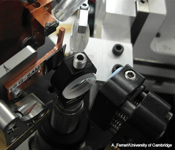 An ultrafast tunable VECSEL in the lab at ETH Zurich uses a single-layer of graphene as a saturable absorber in a 6-cm-long cavity.
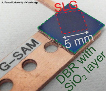 A λ/8 graphene saturable absorber mirror (G-SAM) features a square of single-layer graphene 5 mm across (red dotted line) on a layer of SiO2. The graphene is fabricated on copper and transferred to a quartz mirror in the laser cavity.
In 2009, Andrea Ferrari, professor of nanotechnology at the University of Cambridge, U.K., and colleagues began to demonstrate the practical use of graphene as a mode-locker at several infrared wavelengths. In late 2013, Ferrari’s team demonstrated graphene mode locking at 2 µm in a solid-state laser that generated 410 fs pulses, 270 mW average output power, and 110 MHz repetition rate. The graphene mode-locked laser requires a single layer of graphene inside the laser cavity, enabling a laser that is very compact and tunable. Experiments have demonstrated that the same graphene sample used at 1 µm, 1.3 µm and 1.5 µm is usable at 2 µm.
“This shows how simple it is to introduce a graphene sample inside the laser cavity,” says Ferrari.
Moving toward VECSELs
More recently, in collaboration with Professor Ursula Keller’s group at ETH Zurich, Switzerland, Ferrari’s team has focused on a new generation of mode-locked vertical-external-cavity surface-emitting lasers (VECSELs) using graphene-based saturable absorbers (GSLs). In contrast to the tiny enclosed cavity of a conventional vertical-cavity surface-emitting laser (VCSEL), a VECSEL consists of an external cavity formed by high-reflection mirrors and an output coupler, with a typical cavity measuring a few millimeters to tens of centimeters. The gain chip consists of a highly reflective bottom (to reflect the laser and pump light), an active semiconductor gain section and an anti-reflective top layer.
VECSELs thus combine the advantages of compact semiconductor lasers and diode-pumped solid-state lasers, achieving low timing jitter, excellent beam quality, and high average and peak power. Ultrafast VECSELs (also called semiconductor disk lasers or optically pumped semiconductor lasers) have potential as pulsed sources for multiphoton microscopy, fiber optic communications, supercontinuum generation and ultracompact stabilized frequency combs.
The Ferrari-Keller collaboration has used a GSL to mode-lock a VECSEL from 935 to 981 nm. The VECSEL is widely tunable over that 46 nm band, which makes it the widest-tunable VECSEL reported to date.
The group is considering further applications, such as graphene-based waveguides and nonlinear devices, as well as fiber-based ultrafast lasers. Graphene has other applications in photonics as well, including solar cells, photodetectors and for integration into optical components such as output coupler mirrors, dispersive mirrors and dielectric coatings on gain materials.
Passively mode-locked VECSELs are only a few years old and, according to Dr. Rüdiger Paschotta, the founder of RP Photonics Consulting GmbH, could be poised for significant further advances in performance, especially combining multi-gigahertz repetition rates, multi-watt output powers and sub-picosecond pulse durations. What’s more, the application of wafer-scale technologies may allow very-low-cost mode-locked VECSELs, opening up a range of new applications where cost is a factor.
|
Micromachining: The ultrafast difference
Meanwhile, the commercial use of ultrafast lasers for precise, powerful industrial applications like micromachining and processing is well established on all types of materials, ranging from textiles and polymers to metals and semiconductor wafers. And the advent of ever-shorter, ever-more-stable pulses is enabling more efficient, cost-effective micromachining and is increasing the role of these lasers in other industries. Micromachining with femtosecond lasers can produce repeatable, precise features down to 10 µm in size, like holes and grooves on surfaces or structures. Such tiny structured surfaces might be used in microfluidic devices or a lab-on-a-chip.
Medical stents—the tiny mesh tubes inserted into a natural passage or conduit in the body, such as a blood vessel, to counteract a localized flow constriction, such as arterial blockage—form an interesting case study in comparing nanosecond and picosecond/femtosecond technology.
Stents are conventionally manufactured in metals using Nd:YAG lasers, the pulse duration of which varies from milliseconds to nanoseconds. The longer pulse lengths produce heat-affected zones and melting along the cut edges, and a deposition of solidified droplets stuck to the tube surface. The result: burrs along the cut that can’t easily be cleaned on the smallest of stents, preventing their use in smaller veins. In addition, Nd:YAG lasers aren’t effective at processing all of the potential materials that would be useful for making stents.
Picosecond and femtosecond lasers, in contrast, can overcome this problem through a process called cold ablation. This occurs when intensity of a high-energy laser pulse exceeds the ablation threshold and penetrates more deeply into the material, causing it to sublimate into a plasma and eliminating thermal debris.
Femtosecond lasers that enable cold ablation can produce high-quality stents with no post-processing, not only in metals but also in polymers that degrade naturally over time. Use of lasers with pulse lengths shorter than 12 ps can help to avoid melt debris that could alter the chemistry of the human body when the device is inserted. Such an approach requires more stable pointing, which, if mastered, can drill thicker materials with fewer shots without losing accuracy—useful not just in biomedicine but in other industries requiring high-throughput, precision processing, such as automotive, consumer electronics, mobile displays and 3-D semiconductors.
 (Top) Femtosecond laser technology enables precision engraving of a lab-on-a-chip, which incorporates the functionalities of an entire laboratory onto a single glass substrate. (Bottom left) Femtosecond lasers can engrave precision patterns on tiny objects, such as this 2-mm-diameter stent made of a nickel titanium alloy. (Bottom right) Femtosecond lasers like TRUMPF’s TruMicro 5070 perform micromachining with a negligible heat-affected zone, like this microhole drilled into a printed circuit board substrate.
As always, the choice of pulse length is partly a cost judgment. Femtosecond lasers typically cause less melt, but are more expensive. Laser developer and manufacturer Coherent, based in Santa Clara, Calif., U.S.A., has recently expanded its family of industrial picosecond lasers (based on a modular fiber/regenerative-amplifier technology) with the Talisker HE and RAPID series, whose high-energy pulses, according to the company, enable drilling, cutting and scribing of thicker materials than other ultrafast lasers.
Notes Mark Thompson, senior product manager at Coherent, the Talisker HE and HYPER RAPID-HE lasers are targeted at three different wavelengths with different output options: 200 µJ pulse energy in the near-infrared (1,064 nm) for materials that better dissipate heat, like metals, polymers, glass and ceramics; 120 µJ per pulse in the green (532 nm) for glass; or 40 µJ pulse energy in the ultraviolet (355 nm) for low-melting-point materials like transparent polymers.
“The key spec to achieve is productivity—you want to make quality parts as quickly as possible,” says Thompson. To do that, manufacturers need to concentrate the pulse energy and reduce the spot size, or fluence, to reduce the thermal heating that causes melt debris.
Femtosecond stability
Beyond cost and productivity, says Thompson, another key issue is stability. “Can it withstand 24-7 production in New York during the winter or China in the summer? Can the laser survive international shipping by sea freight? Stability is what distinguishes scientific ultrafast from robust, industrial ultrafast.”
In January 2014, industrial laser manufacturer TRUMPF, based in Farmington, Conn., U.S.A., introduced the TruMicro 5070 femtosecond laser, which is based on its high-power picosecond laser series. The TruMicro 5070 offers pulse durations of 800 ± 200 fs and pulse energy as high as 200 µJ. Featuring repetition rates of 400 and 600 kHz, the new infrared laser emits at 1030 nm with a remarkable 80 W of average output power.
The TruMicro 5070, according to TRUMPF, is designed to provide consistent results in demanding industrial production environments. The system separates pulse generation and pulse emission and uses feedback systems to monitor individual pulses to maintain constant power, pulse energy and duration, and beam quality. Initial applications include drilling holes in circuit boards and processing polymers used in medical implants. According to Sascha Weiler, program manager, Micro Processing, at TRUMPF, these advantages, along with the higher power and shorter pulse duration, “directly translate into throughput, reducing the ‘cost per watt’ and therefore the ‘cost per part.’”
The challenge for commercial femtosecond lasers, according to Weiler, is to translate power into speed while reducing price—an 80W CW laser will be always cheaper than an 80W fs laser. But, says Weiler, the price of ps/fs lasers hinges on economies of scale, so prices should come down as these lasers find more and more applications.
Improving throughput with parallel beams
In addition to pulse speed, maximizing the speed of the production process itself is another challenge in femtosecond micromachining. Conventional material processes scan sequentially over the target, dot by dot. Rotary scan heads can help by moving the beam very quickly from point to point. Another option, however, is to split the original beam into several beams for parallel processing.
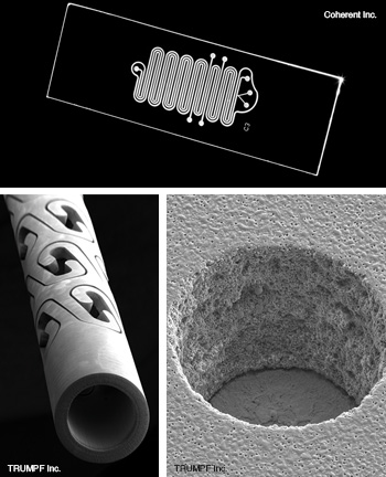
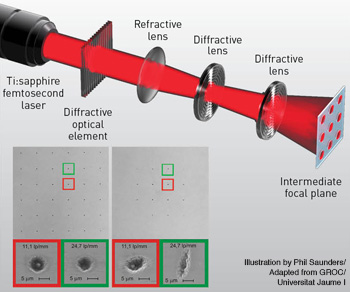 Dispersion-compensated module: (Top) The diffractive-refractive dispersion-compensated module uses a femtosecond Ti:sapphire laser and optics to create multiple beams for improved multifocal micromachining. Optical microscopy reveals the details of the ablated surface of a stainless steel sheet with (bottom left) the dispersion-compensated module and (bottom right) a conventional setup. In the bottom part of the figure, the SEM images of the holes correspond to different diffraction orders.
Researchers with the Group of Research in Optics at Universitat Jaume I (GROC–UJI) in Castellón de la Plana, Spain, recently investigated a promising parallel-processing technique. According to Gladys Mínguez-Vega, associate professor of physics and a GROC–UJI member, a split-beam solution makes sense because it eliminates the extensive attenuation required for current regenerative or multipass amplifier systems, which produce pulse energies in the millijoule range. Furthermore, splitting the beam into an array of multiple beams improves production and throughput, reduces fabrication time and maximizes full use of the laser’s energy.
In the parallel-beam setup, the group used a suited dispersion-compensated module (DCM) to focus the light. Consisting of a diffractive optical element (DOE), one refractive lens and two diffractive lenses, the DCM increased the ablation area by nearly a factor of three. The DCM also mitigated first-order chromatic aberration and pulse stretching on the target material caused by use of DOEs. The setup projected a 30 fs laser pulse in a parallel-processing configuration onto a stainless steel sample to simultaneously create 52 blind holes measuring less than 5 µm across.
“We can increase the speed of manufacturing by a factor of 52—or even more by changing the system parameters—without a loss of quality,” says Mínguez-Vega. “We believe this may be of interest to manufacturers that want a higher throughput of their millijoule laser for micromachining applications.” While the experimental system used expensive diffractive optical elements fabricated on a glass substrate (costing about €4000), the team suggests using polymer materials for cost-effective, high-volume production DOEs.
Banishing microcracks
Another potential application area for such parallel processing is cutting the scratch-resistant cover glass for mobile phones. If the glass is cut by a conventional long pulse, the pulse duration is sufficient to thermally generate microcracks in the material, to the detriment of quality. Femtosecond lasers concentrate the energy in such a short pulse duration that heat cannot be transferred to the surrounding material. The cutting process then becomes truly athermal, and microcracks don’t develop. Many other applications may benefit from industrial processing with precision femtosecond lasers, including patterning of thin-film solar cells, chip manipulation and fabrication of nanoparticles.
The GROC–UJI team next plans to study how to alleviate the mechanical tolerances in femtosecond laser microprocessing. To generate feature size with high quality and small dimensions, the most widely adopted method is to focus the light with a refractive lens. This allows concentration of the beam energy onto a small area, the minimum size of which is restricted by the diffraction limit and the beam aberrations.
In addition, precision micromachining is highly susceptible to minor displacements caused by environmental disturbances such as temperature variation or system vibration. This can be a bottleneck for the fabrication of nanostructures, and micro-processing of rough samples or of large areas where active compensation of sample tilt would be required. Sophisticated monitoring and control of the focal position not only slows the speed of the material processing due to the continuous realignment, but also increases the cost of the beam delivery system. Researchers are currently working hard to obtain stable laser modules with high mechanical tolerances.
“We want to face the problem of alleviating mechanical tolerances in femtosecond micromachining by using diffractive lenses for light focusing instead of the refractive ones,” says Mínguez-Vega. “Due to the strong dependence of the focal length of a diffractive lens on the wavelength of light, a diffractive lens generates a longer focus and the position of the target becomes less critical.”
A complex market
Clearly, developments in both academic and commercial research labs, while defining an exciting array of new possibilities and applications, are making this particular technology space complex and challenging for most customers. The best pulse length, wavelength, peak power, throughput and price for a user constitute a complex set of trade-offs that depend on the application in question. “There is no one ps/fs/ns laser that fits all micromachining applications,” notes TRUMPF’s Weiler. “Material properties, quality, speed and budget requirements all help determine which laser fits best for the application.”
Thompson at Coherent agrees. “A good manufacturing rep will drive the right product to the right application. The processes are high risk with a high return on investment; it pays to build a strong strategic partnership with an expert manufacturer and work closely with them to get the right system for your needs.”
Valerie C. Coffey is a freelance science and technology writer and editor based in Acton, Mass., U.S.A.
