
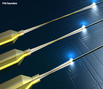
The emerging field of plasmonics promises the generation, processing, transmission, sensing and detection of signals at optical frequencies along metallic surfaces much smaller than the wavelengths they carry. Plasmonic technology has applications in a wide range of fields, including biophotonics, sensing, chemistry and medicine. But perhaps the area where it will have the most profound impact is in optical communications, since plasmonic waves oscillate at optical frequencies and thus can carry information at optical bandwidths.
In plasmonics, the important signal processing step is performed on surface plasmon-polaritons (SPPs) instead of photons. SPPs are electromagnetic waves coupled to charge density oscillations at the interface between a material of negative permittivity and one of positive permittivity (e.g., a metal and an insulator, respectively).
This might sound complicated, but it’s not: It just means that, if a photon oscillating at an optical frequency of 190 THz is irradiated onto a metal-insulator interface, it may pass its energy in part to the electrons at the interface, and the electrons may start to oscillate themselves at that frequency. After signal processing has been performed, the SPPs are converted back to the optical domain. Exciting an SPP with photons is only possible if both energy and momentum conservation are met. This is done by properly choosing the incidence angle and material composition at the interfaces.
 Argishti Melikyan (left), Juerg Leuthold and Sascha Muehlbrandt in the plasmonics lab at the Karlsruhe Institute of Technology.
Plasmonics could be the key to overcoming one of the great challenges in integrated optics—the huge size mismatch between large-scale integrated photonics and small-scale integrated electronics. Modern electronic transistors have dimensions of tens of nanometers, while the size of conventional photonic devices is dictated by the optical wavelength, typically several hundreds of nanometers (λ/2, about 500 nm for telecom frequencies in glass). Also contributing to the disparity is the fact that photonic devices typically have footprints that easily extend over several millimeters.
Fortunately, signals in plasmonic waveguides can have transverse dimensions smaller than 100 nm. Thus, plasmonic devices can help bridge the size gap. They may also speed up optical processing by virtue of their compactness. For instance, electro-optical devices are usually resistor-capacitor (RC)-limited, where the resistance comes from resistive sheets between the metal-contact and the waveguide. In plasmonic devices, however, the waveguides are metal contacts, and the resistance can be made arbitrarily small. Therefore, an electrically operated plasmonic device should not be speed-limited—if it were not for RC limitations in the driver circuit. Last but not least, intensities in plasmonic waveguides are very strong due to the small cross-section, and thus plasmonic nonlinear devices are possible within shorter devices and with lower optical powers.
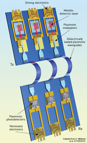 CMOS chips with integrated driving electronics at the outputs feed their signals directly into a plasmonic modulator, which encodes the electrical signal onto a surface plasmon polariton. The signal is then transmitted over a dielectrically loaded plasmonic waveguide and received in a plasmonic photodetector.
Given their large bandwidth and compact size, plasmonic devices are of particular interest in applications where speed, footprint, CMOS compatibility and price matter—for example, for chip-to-chip interconnects used in short-range communication. But before plasmonic communication systems can be realized, the device “toolbox” needs to be filled with compact and functional waveguides, lasers, modulators, detectors and amplifier devices—all of which are needed to build a transceiver.
Plasmonic waveguides
Plasmonic waveguides come in a variety of shapes and offer different levels of confinement.
The simplest structure is the metal-insulator interface. The SPP propagates along the interface; its power peaks at the interface and decays exponentially into the adjacent materials. As a significant portion of the optical power is in the metal, the plasmonic signal suffers significant decay. Propagation lengths in this case are typically on the order of microns or tens of microns.
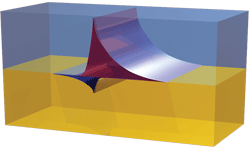
Other simple but important 1-D waveguides are made of three layers. The insulator-metal-insulator (IMI) waveguide has a long-range SPP with propagation lengths that can reach centimeters under the right conditions. IMI can offer increased propagation lengths for thin metal films or high confinement for thick metal films. For very thick metal films, an IMI behaves like two separate metal-insulator waveguides. The metal-insulator-metal waveguide provides superior confinement, as the signal tails decay sharply in the metals.
Waveguide guidance is provided by laterally structuring the layers. Several waveguide concepts are described in the literature, including the dielectrically loaded waveguide (which offers versatility through careful choice of the dielectric ridge), the metal stripe waveguide (which allows for a simple end-fire excitation) and the channel waveguide (which offers good confinement for relatively long propagation lengths).
|
There is a trade-off between high energy confinement with high losses and long propagation lengths, but it can be circumvented by using different geometrical designs or materials. It is also possible to increase propagation lengths by introducing amplification within the materials.
Plasmonic lasers and metal-cavity nanolasers
Electrically pumped semiconductor nanolasers with metallic cavities are among the most compact lasers. They have generated a lot of interest because of their potential for high-integration density, low-current operation, ultra-fast modulation and immunity to cross-talk.
The first experimental demonstration of an electrically pumped laser with a metallic cavity showed continuous lasing around 1,400 nm with a threshold current of 6 μA at 77 K. It was a cylindrical semiconductor pillar with a height of 1.6 μm and a diameter of about 250 nm, consisting of an InGaAs active medium sandwiched by InP pillar sections, surrounded by a thin insulating Si3N4 layer and followed by a silver cladding. The metallic cavity acted as the n-contact itself, and a lateral p-contact deployed over a larger area was included to minimize the electrical resistance of the device. This idea was further extended to fabricate Fabry Perot and distributed feedback plasmonic lasers, based on metal-insulator-semiconductor-insulator-metal waveguides.
Later, researchers proposed several metallic cavities: a nanopatch laser able to radiate laterally; a metal-coated ring resonator; a metallo-dielectric laser that supported a dielectric mode and used the metallic cladding as a mirror to provide strong feedback (allowing pulsed lasing at room temperature); and a subwavelength-cavity laser with continuous wave operation at room temperature.
Current focus is on coupling the emitted light directly into a waveguide using the evanescent field and butt coupling. Scientists are also working on coupling a III-V metallo-dielectric nanopillar laser to a Si/SiO2 waveguide. The approach lies in using a metallo-dielectric cavity laser supporting a dielectric transversal-electric polarized mode, which is coupled to a waveguide in an InP membrane bonded with benzocyclobutene to silicon for compatibility with silicon photonics and CMOS. In a second step, the InP-waveguide is coupled to an underlying silicon waveguide by means of a linear taper, as has been demonstrated in other III-V lasers bonded to silicon. The metallo-dielectric laser combines very compact dimensions with better lasing properties than a purely plasmonic laser.
Plasmonic modulators
These encode electrical signals onto SPPs and then transform the information back into an optical signal. They boost the electrical-plasmonic interaction by strongly confining their fields in a small active region of the modulator. The ultra-compact dimensions of plasmonic modulators also help to overcome speed limitations such as those imposed by RC-constants or the walk-off between electrical and optical waves in conventional devices.
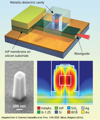 (Top) A metallo-dielectric nanolaser coupled to an InP-membrane waveguide is able to provide up to 100 µW of output power, according to simulations. (Bottom, left) SEM image of a semiconductor pillar intended to form the laser cavity. (Bottom, right) Cross-section showing the evanescent coupling between the pillar laser and the waveguide. The modulus squared of the electric field distribution is shown in logarithmic scale.
Researchers have proposed several approaches to creating plasmonic modulators that vary either the phase or intensity of a plasmonic wave. They recently demonstrated an SPP absorption modulator (SPPAM) by exploiting high optical losses in a charge-accumulated metal-oxide layer when applying an electrical field. The SPPAM device consists of a stack of metal-oxide insulators that is tens-of-nanometers thick and sandwiched between two metals. The metal-oxide is highly conductive and transparent. The structure is capable of guiding a hybrid plasmonic mode, where the optical fields’ maximum occurs at the metal-oxide-insulator interface. The insulator is needed to electrically separate the bottom and top metal so that an external voltage can be applied between them.
A negative bias on the electrode leads to a charge carrier density increase in the conductive metal-oxide by several orders of magnitude, allowing the complex refractive index and the optical losses of the guided mode to be tuned. By applying an electrical signal to the electrodes, the intensity of light passing through the device can be modulated. In a variation on this design, the bottom electrode is replaced by a doped silicon layer that creates extinction ratios of 1 dB per µm of device length; this has been demonstrated in a wavelength range spanning 1.2 to 2.2 µm, while the insertion loss was on the order of −1 dB for a 5-µm–long device.
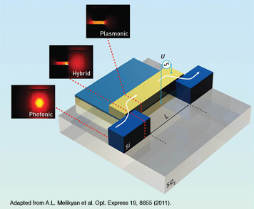 Light is coupled from a silicon nanowire into an active plasmonic section by means of a directional coupler. The insets show how a photonic mode in a silicon strip waveguide excites an SPP via a hybrid mode in a directional coupler. The SPP guided through the device with a length L is modulated by the external voltage with a voltage swing of U.
Plasmonic photodetectors and amplifiers
Photodiodes work on a two-step principle: A light field incident on a photo-responsive material induces an electrical oscillation, which is then rectified. Conventional photodiodes exploit absorption in a semiconducting material, creating charge carriers that induce a measurable current when a field is applied. Devices based on this scheme have already demonstrated bandwidths beyond 100 GHz. Compared to electronics, such detectors tend to be relatively large and will always be limited in speed as a consequence of inherent RC limitations in the absorption layer.
In an attempt to reduce RC limitations, researchers have introduced novel plasmonic coupling schemes that allow for much smaller dimensions. When a plasmonic grating or antenna is used, the photodiode shrinks to subwavelength dimensions. The metal nanostructures themselves generate free carriers by internal photo-emission at a metal-semiconductor interface of sub-wavelength optical antennas. Up to now, such approaches lacked sufficient quantum efficiencies, and benefits were only achieved with respect to the size of single devices. Therefore, high-speed plasmonic detectors with a large responsitivity comparable to conventional photodiodes remain a challenge.
Alternatively, researchers are investigating detectors based on a conductive layer of quantum dots (QDs). One detector concept consists of an amplifying section in combination with a photodetector. In the first part of the chip, the plasmonic amplifier contains a gold nanostripe surrounded by a polymer with active centers. This polymer acts as a dielectric with gain that is able to compensate for the losses of the gold waveguide when the active centers were either optically or electrically pumped.
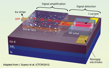 The plasmonic amplifier (on the left) consists of a gold (Au) nanostripe surrounded by a polymer with active centers inside (SU-8+QDs). The polymer acts as a dielectric with gain that can compensate for the losses of the gold waveguide when the active centers were optically or electrically pumped. The photodetector (on the right) consists of a 100-nm–thick conductive layer of PbS quantum dots (QD solid) that generates an electrical current in response to the incoming photons.
The photodetector is made of a 100-nm–thick conductive layer of lead sulfide (PbS) QDs that can generate an electrical current in response to the incoming photons. Reported responsivities in recent literature is in the range of 0.1–3.9 A/W for a PbS QD monolayer in a nanogap photoconductor; larger than 100 A/W for a PbS layer thicker than 200 nm; and more than 106 A/W in a metal-oxide-semiconductor structure based on a PbS layer (60 × 80 nm thick) on graphene. The QD-solid approach is considered a new and advanced concept for photodetection, given the high absorption of QDs, the low cost of the solution-processing technique used to deposit the material and its integration in silicon technology. Furthermore, this concept can be easily combined with plasmonic layers based on metal nanoparticles, because a responsivity enhancement is expected due to the light trapping effect at the band edge of the QD-solid.
What the future holds
New plasmonic devices are coming. They can be 100 times smaller and 1,000 times faster than current photonic devices. If we can fill the plasmonic “toolbox” and optimize performance, we will enjoy ultra-compact, integratable plasmonic transceivers with footprints of 1–100 µm2. At first, these devices may be used in novel highly integrated chip-to-chip interconnects. But as soon as we can overcome the high loss bottleneck, plasmonic devices will make their way into state-of-the-art wavelength-division multiplexing systems—and perhaps a new plasmonic revolution will begin.
J. Leuthold is with the Swiss Federal Institute of Technology (ETH), Zurich, Switzerland, and the Karlsruhe Institute of Technology (KIT), Karlsruhe, Germany. C. Hoessbacher is with ETH. S. Muehlbrandt, A. Melikyan, M. Kohl, C. Koos and W. Freude are with KIT. V. Dolores-Calzadilla and M. Smit are with the Eindhoven University of Technology, Netherlands. I. Suarez and J. Martínez-Pastor are with the University of Valencia, Spain. E.P. Fitrakis and I. Tomkos are with the Research and Education Laboratory in Information Technologies (AIT), Athens, Greece.
