
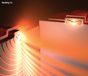
 Plasmonic structures shape semiconductor laser beams. Left: A plasmonic collimator spreads out radiation from the sub-wavelength aperture into surface waves that are diffracted by the metallic grating to produce a low divergence beam. Right: A resonant optical antenna concentrates most of the laser light into a tens-of-nanometers size spot defined by the gap.
In nanophotonics, light is controlled using metallic and dielectric nanostructures with feature sizes much smaller than a wavelength. The first modern application of nanophotonics was probably the near-field scanning optical microscope. But there is also historical evidence that ancient Greek and medieval artisans unwittingly used nanophotonics to impart bright colors on glass objects; the glass had been doped with metallic nanoparticles that caused it to absorb and scatter light at certain wavelengths.
Absorption in metallic nanoparticles is caused by confined collective oscillations of electrons interacting with an electromagnetic field, known as surface plasmon resonances. Surface plasmons can also propagate along the interface between a metal and a dielectric as electron density waves coupled to the electromagnetic field. Researchers have known about plasmons for decades, but it wasn’t until recently that they began integrating plasmonic structures onto common optical components, such as semiconductor lasers and optical fibers, in order to engineer their near- and far-fields and create new functionalities.
The manipulation of light using surface plasmons—known as plasmonics—has a wide range of applications in imaging, sensing, communications and optical manipulation. Unlike conventional optical components, plasmonic structures manipulate light at the sub-wavelength level in real space or over a wide range of k vectors in wave-vector space.
Our work explores the use of plasmonics for laser beam shaping based on monolithic integration. Currently, laser beams are manipulated externally using optical components such as lenses, beam-splitting polarizers and wave plates. These components are often bulky and expensive and don’t provide the degree of flexibility and the range of new functionalities made possible by integrated optics.
Plasmonics could provide a compact and universal solution to beam shaping for semiconductor lasers and optical-fiber-based light sources. By fabricating in situ on their facet sub-wavelength metallic-dielectric structures, researchers can design the near-field and far-field almost at will to achieve major performance improvements or to add new functionalities.
Semiconductor lasers now permeate our society, as key components in widespread commercial technologies such as optical fiber communications and CD and DVD players. However, their beams usually have a large divergence angle (of around tens of degrees) due to the significant diffraction caused by the small emission aperture of the devices. In addition, light output is mostly linearly polarized along a single direction, which is determined by the optical selection rules of the gain medium.
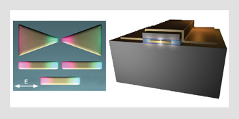 Resonant optical antenna designs. Left: The antenna resonance condition leads to a strong near-field enhancement at the antenna ends with respect to the incident field (bottom). The coupled-rods design (middle) is used to create highly localized, well-defined light spots at the central antenna gap. The bow-tie design (top) maximizes field concentration in the nanogap compared to the outer ends of the antenna segments. Pink and bright cyan stand for positive and negative charge distributions in the antennas, respectively. Resonant optical antennas can capture a light beam with a cross-section much larger than their geometrical size. Right: A semiconductor laser with a resonant optical antenna integrated on the facet.
Clearly new beam-shaping schemes could improve myriad technologies by greatly reducing beam divergence and by making available a wide range of polarization states, such as circular polarization and linear polarization along different directions. Such a feat would be technologically important. Specifically, we can envision collimators and polarizers consisting of metallic gratings, apertures, antennas or other configurations. Another challenge is to concentrate laser light in regions much smaller than the wavelength—which would dramatically improve the information capacity of optical disks. In this article, we address some of these questions in detail and demonstrate specific solutions.
Plasmonic laser antennas
A variety of strategies have emerged that take advantage of localized near-fields that are generated by suitably shaped metallic nanoparticles known as optical antennas. Optical antennas can produce very high near-field intensities when their size is properly matched to the wavelength of the incident light. This resonance condition is achieved when the length of the antenna segments is chosen to be approximately half the wavelength of surface plasmons excited in the metal by the incident radiation and the latter is polarized along the antenna length.
Recently, there has been a great deal of scientific interest in the use of active optical devices that can generate sub-wavelength optical spots for various applications. Researchers have demonstrated very-small-aperture lasers that consist of a laser diode with its facet coated by a metal film on which a sub-wavelength hole is etched by focused ion beam milling. However, these and related devices suffer from limited throughput, since the transmitted power scales strongly with the hole diameter (with the fourth power through a sub-wavelength hole in a perfect metal).
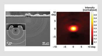
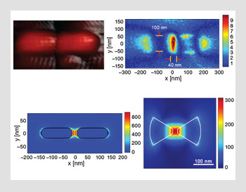 Simulation and experimental results of laser antennas. Top: Atomic force microscope topography (left) and near-field scanning optical microscope image (right) of a resonant optical antenna fabricated on the facet of a λo=0.83-µm diode laser. Color coding is arbitrary. Bottom: (Left) Numerical simulation of the optical intensity enhancement with respect to the incident intensity at λo=0.83 µm. (Right) Map of optical intensity enhancement for a bow-tie optical antenna designed for a vertical-cavity surface-emitting laser emitting at λo=0.85 µm.
Plasmonic laser antennas, which consist of a resonant optical antenna integrated on the facet of a semiconductor laser, don’t suffer from this problem. Resonant antennas indeed can capture a substantial part of the power of the incident laser beam and concentrate it into a spot the size of the nanometric antenna gap, leading to a light intensity hundreds or even thousands of times stronger than that of the incident beam. Such a compact laser source with sub-wavelength spatial resolution could provide distinct advantages in a number of applications, including microscopy, spectroscopy, terabyte-level optical data storage, lithography and laser processing.
We fabricated an optical antenna that comprises a pair of gold nanoparticles on the facet of a commercial near-infrared edge-emitting laser diode (Sanyo, Inc.). A thin silicon dioxide insulating layer separated the metal from the facet to avoid electrical shorting. We used an aperture-less near-field scanning optical microscope to map the optical near-field distribution in the fabricated devices.
In this technique, a nanoscale sharp gold-coated atomic force microscope tip, driven at its resonant frequency, scatters the light from the near-field as it scans over the sample. The weak light back-scattered into the laser is collected by the back-facet photodiode incorporated in the laser package, thus providing a two-dimensional map of the near-field, as shown in the top figure on the right. This device is capable of generating an intense optical spot (~100 MW/cm2 at a distance of 10 nm above the center of the antenna) that is localized within an area 50 times smaller than what one would obtain with conventional diffraction-limited optics such as lenses.
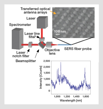 Antenna arrays on optical fiber facet. (Top) Configuration used to collect signal from the surface-enhanced Raman scattering (SERS) fiber probe. The spectrometer measures the SERS signal from analytes interacting with optical antennas transferred to a fiber facet (inset). (Bottom) Benzenethiol remotely detected through its SERS spectrum measured with the fiber sensor.
We have also demonstrated plasmonic laser antennas with 100-nm size spots at mid-infrared wavelengths using quantum cascade lasers. This work opens up intriguing opportunities for sub-wavelength chemical-biological imaging—of a cell’s interior, for example.
Optical antenna arrays fabricated at the end of an optical fiber can be used for detecting molecules with surface-enhanced Raman scattering. Here, the strong near-fields of the coupled antennas lead to an enhancement of the Raman signal by many orders of magnitude, since both the incident laser field and the Stokes field are resonantly enhanced.
This device could have important applications for in situ chemical sensing in remote locations and microfluidic environments. Also, the fabrication of the array required us to develop a powerful new soft-lithography technique to transfer nanoscale patterns that had been defined by e-beam lithography. Soft lithography has a unique potential to be used for nanoscale patterning of unconventional and non-planar substrates.
Plasmonic collimators: small divergence lasers
Thomas Ebbesen of the University of Strasbourg and coworkers have systematically studied experimentally and theoretically the high directional emission from a sub-wavelength aperture surrounded by surface corrugations. Our plasmonic collimators are based on these findings. They work by coupling laser emission from a sub-wavelength aperture into surface plasmons propagating along the laser facet patterned with a second-order grating. Radiation from the grating groves and the aperture interfere constructively in the far-field, leading to greatly reduced divergence compared to the unpatterned laser.
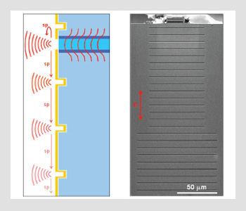 1D plasmonic collimators. (Left panel) Cross-section of 1D plasmonic collimator fabricated on a semiconductor laser facet. A thin dielectric electrically isolates the metal film from the facet. Light waves diffracted by the sub-wavelength aperture and the grating grooves constructively interfere in the far-field to produce a low divergence beam in the vertical direction. (Right panel) Electron micrograph of the facet of a patterned mid-infrared quantum cascade laser emitting at λo=10 µm.
The 1D plasmonic collimator consists of a slit aperture and a grating patterned on the metal-coated laser facet. The slit aperture and the grating grooves are oriented to be perpendicular to the laser polarization. The aperture slit couples part of the laser output into surface plasmons, which propagate through the grating along the vertical direction and are scattered by the grating grooves as outgoing radiation. The separation between the aperture slit and the grating and between the grating grooves are chosen to ensure maximum constructive interference in the far-field in the direction normal to the facet, leading to a strong reduction in the beam divergence along the vertical direction. The grating period is comparable to the wavelength, while the grooves’ widths and depths are sub-wavelength.
Effectively, the aperture and the grooves in the plasmonic collimator act as an array of coherent light sources, in analogy with phased array antennas. The divergence in the vertical direction is reduced by more than a factor of 20 with respect to the same device before patterning—in very good agreement with the simulations, as shown in the panel “Simulated and measured far-fields of 1D collimator.”
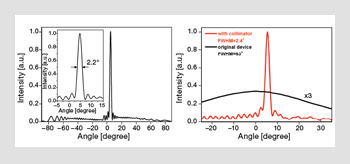 Simulated and measured far-fields of 1D collimator. (Left) Simulated far-field in the vertical direction, including zoom-in view of the dominant lobe for a device with 24 grooves emitting at λo=10 µm. (Right) Measured far-field of the patterned laser (right side of figure above) in the vertical direction (red curve) and of the unpatterned laser (black curve) showing a reduction of the vertical divergence angle from about 60° to 2.5°. The central lobe of the far-field of the patterned devices contains about 70% of the total output power, which is comparable to that of the unpatterned device (peak value ~120 mW).
Since mid-infrared surface plasmons are capable of propagating over long distances of a few millimeters along unpatterned gold-air interfaces, hundreds of grating grooves can be used to couple most of the energy of the plasmons back into free space. The power throughput of the device can therefore be preserved while the divergence angle is simultaneously reduced. Collimators and other devices for beam engineering based on surface plasmons can be used down to near-infrared wavelengths. At visible wavelengths, on the other hand, the shortcomings of increased optical losses will limit the collimation effect and power throughput. For example, at visible wavelengths, surface plasmons can only propagate a distance comparable to 100 wavelengths, which is one order of magnitude smaller than their mid-infrared counterparts.
The grating discussed so far extends only along the laser polarization direction. The lateral dimension of the slit aperture is several times larger than the free space wavelength λo, so that surface plasmons propagate mainly in the direction perpendicular to the aperture slit; as a result, beam collimation is only realized in one direction.
To achieve collimation in the entire beam cross-section, we designed an aperture that can launch surface plasmons in two dimensions and created a two-dimensional plasmonic collimator that can coherently scatter the surface plasmon radiation into the far-field. This leads to constructive interference in both the vertical and lateral directions, thus achieving excellent collimation in the plane perpendicular to the laser beam.
 2D collimation. (Left) Electron micrograph of the facet of a λo=8.0-µm wavelength quantum cascade laser patterned with a 2D plasmonic collimator. (Right) Measured 2D far-field intensity profile for the device demonstrating a major reduction in beam divergence by a factor of ~30 and ~10 in the vertical and lateral directions, respectively, compared to the original unpatterned laser.
Several plasmonic structures can satisfy these requirements; we chose a relatively simple design consisting of a rectangular aperture and a concentric half-ring grating. We performed a detailed study for patterned quantum cascade lasers with λo=8.06 µm. A sub-wavelength rectangular aperture (10 µm2 area) is positioned in the center of the active region. The grating period is comparable to the wavelength, while the grooves’ widths and depths are sub-wavelength, as shown in the left side of the panel “2D collimation.” There was a dramatic improvement in collimation, as demonstrated by the large reduction in beam divergence shown in the right side of the panel “2D collimation.” The beam quality factor (M2 factor) of a device with 20 rings is about 2.0 in both the vertical and lateral directions.
Plasmonic control of polarization
Plasmons can be used to control semiconductor laser polarization by means of metallic gratings and sub-wavelength apertures patterned on the laser emission facet. An integrated plasmonic polarizer can project the polarization of a semiconductor laser onto other directions. Alternatively, a circularly polarized laser beam can be achieved by designing a facet with two orthogonal grating-aperture structures.
To project the laser polarization onto a direction defined by θ, we used an aperture-grating plasmonic structure similar to that of the one-dimensional collimator, except that here the normal to the slit aperture and the grating grooves is at an angle θ from the vertical direction. Only the component of the laser polarization perpendicular to the aperture slit couples to surface plasmons propagating along the grating. The output of the device is thus an interference pattern produced by direct emission from the aperture and coherent scattering from the grating grooves due to Bragg diffraction of surface plasmons by the second-order grating. The polarization of the reemitted light is along the θ direction, determined by the orientation of the grooves.
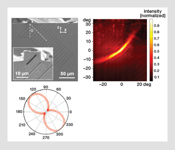 Plasmonic polarizer. Top: (Left) Electron micrograph of the facet of a λo=10-µm quantum cascade laser patterned with a plasmonic polarizer that can project the vertical polarization of the original laser onto the 45° direction. (Right) Measured 2D far-field intensity profile for the device. Beam divergence is reduced along the 45° direction. Bottom: A wire-grid polarizer was used to determine the beam’s polarization state. As its axis is rotated, the maximum optical power was detected for orientation normal to the grating grooves, with a high polarization suppression ratio. Red circles are experimental data.
The right panel of the figure “Plasmonic polarizer” shows that the grating greatly reduces the beam divergence angle along θ=45° direction due to the interference effect. By detecting the power transmission of the device output through a conventional wire-grid polarizer, we found that the polarization of the main lobe of the far-field is essentially linearly polarized along the 45° direction.
A circularly polarized laser could find many applications, ranging from the spectroscopy of chiral molecules to satellite communications and quantum information processing. A circularly polarized laser beam can be constructed by coherently combining two linearly polarized beams satisfying three conditions: The two beams should have perpendicular polarizations, a 90° phase difference, and the same amplitude. These conditions can be met by defining two orthogonal aperture-grating structures on the device facet. By tailoring the separations between the aperture and the nearest groove in the two aperture-grating structures, we can control the respective phase and amplitude of the scattered light from the left grating and from the right. Note that direct emission from the apertures into the far-field must be blocked through suitable design.
Looking forward
There are rich opportunities in far- and near-field engineering with plasmons, from both scientific and technological points of view. Some of the challenging questions that scientists face moving forward include: Is it possible to integrate plasmonic structures into lasers to achieve sub-wavelength focusing in the far-field? Can we use plasmonics to create special beams such as Bessel beams, which are diffraction-free beams? What about beams that are radially or azimuthally polarized, or beams with orbital angular momentum, which can be used to rotate small particles?
Another issue of substantial conceptual and practical interest is whether researchers can determine, from a prescribed “designer wavefront,” the sub-wavelength structure that is required to generate it.
Semiconductor lasers and single-mode optical fibers can be viewed as the “optical benches” on which an entire plasmonic network—consisting of surface plasmon waveguides and active/passive nodes (metallic and core-shell nanoparticles, nanocrystals, quantum dots, etc.)—can be built to perform local optical processing. In addition, plasmonic beam shaping can be applied to the optical trapping of nanoscale particles. (Ken Crozier at Harvard is pursuing this line of research.) Finally, using materials with a negative-refractive index fabricated on the facet of laser diodes and fibers, researchers and engineers will be able to create light sources with sub-wavelength focusing in the far-field as well as other interesting functionalities.
The authors acknowledge the following people who also contributed to the work reported in this article: E.A. Kort, K.B. Crozier, M.D. Dickey, J. Bao, G.M. Whitesides, R. Blanchard, J. Fan, Q.J. Wang, C. Pflügl, L. Diehl, T. Edamura, S. Furuta, M. Yamanishi, and H. Kan. The authors would like also to acknowledge funding and support from NSF, AFOSR MURI, DRAPA, NIH, Center for Nanoscale Systems (CNS) at Harvard University, and Hamamatsu Photonics.
Federico Capasso, Nanfang Yu and Elizabeth Smythe are with the School of Engineering and Applied Sciences at Harvard University, Cambridge, Mass., U.S.A. Ertugrul Cubukcu is with the physics department at the University of California, Berkeley, Calif., U.S.A.
References and Resources
>> J. Durnin et al. Phys. Rev. Lett. 58, 1499 (1987).
>> S. Oldenburg et al. Chem. Phys. Lett. 288, 243 (1998).
>> A. Partovi et al. Appl. Phys. Lett. 75, 1515 (1999).
>> J.B. Pendry. Phys. Rev. Lett. 85, 3966 (2000).
>> H.J. Lezec et al. Science 297, 820 (2002).
>> K.B. Crozier et al. J. Appl. Phys. 94, 4632 (2003).
>> L. Martín-Moreno et al. Phys. Rev. Lett. 90, 167401 (2003).
>> M. Padgett et al. Physics Today, 35–40 (May 2004).
>> H.A. Atwater. Sci. Am. 296, issue 4, 56 (2007).
>> R. Merlin. Science 317, 927 (2007).
>> R. Zia et al. Nature Nanotech. 2, 426 (2007).
>> E. Cubukcu et al. IEEE J. Sel. Top. Quantum Electron. 14, 1448 (2008).
>> N. Yu et al. Nature Photon. 2, 564 (2008).
>> N. Yu et al. Appl. Phys. Lett. 93, 181101 (2008).
>> E. Schonbrun et al. Appl. Phys. Lett. 92, 071112 (2008).
>> E.J. Smythe et al. ACS Nano 3, 59 (2009).
>> N. Yu et al. Appl. Phys. Lett. 94, 151101 (2009).
