
 Sheila Hurtt, an epitaxy and materials engineer at Infinera, studies a microscope image of a photonic integrated circuit.
Fiber optics is one of the most crucial aspects of modern communications. Data transmission through optical fiber is very efficient over long distances (up to thousands of kilometers), and a single fiber can carry multiple data streams represented by different wavelengths of light simultaneously.
However, there are some bottlenecks on the information superhighway. In order to build an optical transport system, many components are needed, and each of them must be optimized independently and then combined into a system by an optical fiber connection. Lasers provide the source of coherent light at the wavelength needed for efficient transmission; modulators encode the data (in the simplest case, as “1”’s and “0”’s) onto the transmitted light by modulating the amplitude (intensity) of the light at a rate up to many billions of bits per second (Gb/sec); detectors convert the optical signal to electronic data streams; and other components—including splitters, combiners, amplifiers and attenuators—route and further refine the data signals.
As the Internet drives further demand for fiber capacity, the disadvantages of a discretized architecture have become glaring—namely, the cost, complexity and reliability risk associated with many independent components and couplings. There is also the inability to scale such an architecture. For example, assume bandwidth grows at 75 percent annually (the current growth rate of many networks) for 10 years. Using today’s discretized systems, or even the discretized systems targeted for commercial introduction in the next five years, the Internet would require millions more line cards, thousands more engineers to install them, and it would consume more than 3 gigawatts of electricity—the equivalent of seven new midsized power plants. With the budget constraints faced by telecom companies, this is clearly not a sustainable scenario. However, the introduction of large-scale photonic integrated circuits into telecom networks heralds an alternative approach to building scalable networks.
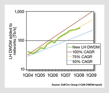 Bandwidth growth (worldwide long-haul DWDM) over the past four years. CAGR=compound annual growth rate.
Researchers have long dreamed of integrating optical components into monolithic optoelectronic integrated circuits (OICs) or photonic integrated circuits (PICs) (see, for example, Miller, 1969), allowing for continued density scaling similar to that in the silicon microelectronics industry and for greater flexibility in network architecture. However, integrating optical communications components poses significant challenges, due to the diversity of components and functions required for creating, modulating, detecting and routing light; the relatively immature state of indium phosphide manufacturing technology; and the limitations on scaling set by the fixed optical wavelength (which is large relative to electron wavelengths in electronics). As a result, progress in optical integration has been slow, even as the rate of microelectronics scaling has been increasing according to Moore’s Law.
Researchers took the first steps toward InP integration in the late 1980s and early 1990s, when several Japanese companies (NTT, NEC and Hitachi, among others) pioneered the electroabsorption modulated laser (EML). It consisted of two discrete components (modulator and laser) on a single chip. These chips enabled very high data rate transmission, and early development (Kawamura, 1987; Soda, 1990) led quickly to commercialization (Aoki, 1991).
More recently, the level of InP integration increased to three or four devices per chip, with the realization of widely tunable transmitters that integrated multi-section sampled-grating lasers with on-chip semiconductor optical amplifiers. Here, too, development at institutions and companies—including UC Santa Barbara, Agility Communications and Bookham, among others—led rapidly to commercialization (Mason, 1999; Akulova, 2002; and Ward, 2005).
Establishing commercial viability for more complex integration schemes has proven to be a significant challenge. Researchers took a key step forward when they invented frequency-selective arrayed waveguide gratings (AWG) filters. These were developed at the Technical University at Delft, at NTT and at AT&T Bell Labs (Smit, 1988; Takahashi, 1990; Dragone, 1991). Using this technology alongside arrays of both transmitters and receivers, researchers have made substantial progress toward developing more complex chip architectures at a number of institutions. Examples of key demonstrations include multiple-wavelength high-speed laser chips, in which multiple signals are multiplexed into a single-output, multi-wavelength modulation, and wavelength selection and conversion.
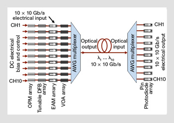 100 Gb/s transmitter and receiver chips. In this block diagram, the TX chip consists of 10 tunable lasers, 10 x 10 Gb/s electro-absorption modulators (EAMs), and 10 variable optical attenuators (VOAs), all coupled to an arrayed-waveguide grating (AWG) multiplexer. In addition, 10 optical power monitors (OPMs) are also integrated monolithically on the transmitter chip. The RX chip consists of 10 x 10 Gb/s high-speed photodetectors coupled to an AWG demultiplexer.
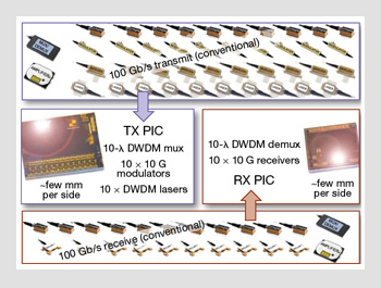 Micrographs of the Infinera transmitter (TX) and receiver (RX) PICs (a few mm on a side), compared with all the discrete components they replace (several cm per component).
This and related research has established a solid foundation for InP-based integration technology and continues to provide innovation in the field. Another potential route to the realization of integration in communications is the development of transmitters and modulators on silicon substrates; this work offers the hope of leveraging the very sophisticated materials integration technology available on Si substrates. However, while researchers have achieved significant milestones at Intel (Rong, 2005) and Stanford University (Kuo, 2005; Roth 2008), they have demonstrated only limited basic functionality of discrete devices to date, and the path to commercialization is uncertain.
In 2004, Infinera deployed monolithic InP-based large-scale PICs with more than 50 discrete components in live telecom networks—a milestone that established commercial viability for InP-based large-scale PICs. The transmitter (TX) chip outputs 10 channels of 10 Gb/s NRZ (non-return-to-zero) optical signals, each converted from electronic inputs using an array of EMLs and multiplexed into a single output fiber, and the receiver (RX) chip outputs 10 channels of 10Gb/s electronic signals, converted from optical signals that are demultiplexed from a single input fiber using an array of waveguide photodetectors.
The figure above on the right shows the block diagram of these OICs. The TX chip contains more than 50 optical components monolithically integrated onto a single InP chip that is smaller than a human thumbnail. The RX chip is even smaller, and it uses more than ten discrete, highly functional components. The impact of this integration is illustrated in the bottom figure on the right, which shows these PICs alongside the discrete components that they replace.
These OICs have demonstrated the performance requirements of a digital transport network system, enabling a big step forward in network flexibility and cost reduction. They also meet the stringent reliability criteria for telecommunications networks: So far, the OICs have accumulated more than 130 million field hours with zero failures, and they have achieved a FIT rate (the standard industry metric for Failures in Time) that exceeds industry expectations for single discrete optical components.
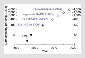 PIC capacity scaling history and roadmap. Scaling of InP-based transmitter photonic integrated circuits in telecommunications networks.
Integration complexity and scaling to meet network growth
Now that large-scale PICs have been demonstrated, we can make scaling predictions for photonics-based chips that are akin to Moore’s Law for microelectronics. In February 2008, Infinera announced a roadmap for photonic integration, predicting the doubling of chip capacity every three years for the next 10 years. PICs have been shown in lab demonstrations to follow the next stage of the roadmap, but new technologies will be needed for photonic integration to continue to scale to a “photonic Moore’s Law” and meet the growing network capacity demand.
To understand this evolutionary path, it is helpful to review modulation formats in optoelectronic devices. Traditionally, optical chips use a standard modulation format known as NRZ, based on on/off keying (OOK), to generate binary data in an optical fiber. In early modulation approaches, engineers used lasers that were directly modulated up to a few Gb/s. However, the electrons and holes that create gain in a laser diode destabilize laser gain at rates greater than 1.0 to 2.5 Gb/s, degrading the quality of the signal in long-haul transmission applications (>80 km). For 10 Gb/s long-haul applications, electro-absorption modulators with integrated lasers (EMLs) represented the first small-scale component integration on a chip.
EMLs modulate a dc-powered diode laser by applying a modulated electric field to a waveguide that contains a reverse-biased diode; this absorbs and extinguishes light traveling through the waveguide, converting continuous laser output into an encoded binary string. The EML is a fundamental building block for a large-scale TX PIC. It has achieved an aggregate data rate of up to 1.6 Tb/s in a chip composed of 40 channels (each at 40 Gb/s). However, simply increasing the NRZ modulation data rate is not a viable path for next-generation networks, since optical signals modulated faster than 20 Gb/s are known to suffer nonlinear penalties over long distances due to dispersion and distortion in the fiber.
Advanced modulation formats are required to extend per-wavelength data rates to 40 Gb/s and beyond for recoverable data transmission over large distances. Simple OOK modulation formats must give way to the encoding of more than just a 1 or a 0 per bit. One way to increase the capacity is to phase-modulate continuous beams of the same laser and detect them by appropriate separation of the phases prior to detection. This way, multiple data streams may be encoded on the same wavelength at the same data rate and power level. Another way is to use polarization multiplexing, where the laser is split and encoded in orthogonal TE and TM components, doubling the data rate with a minor penalty from cross-talk.
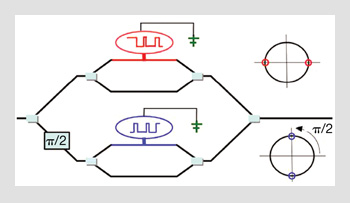 Nested Mach-Zehnder modulator used in DQPSK optical data transmission systems. Light can be split into four equal paths and modulated in two different data streams in this example. To achieve phase quadrature, one branch needs to be rotated a quarter-turn (or π/2).
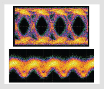 Signal eye diagrams. (Top) A 21.5 Gb/s electrical signal eye modulates the arms of a Mach-Zehnder interferometer in a DQPSK transmitter. (Bottom) A 43-Gb/s DQPSK signal eye received from a transmitter PIC. Constituent 21.5 Gb/s data streams are normally extracted from this signal separately in the receiver PIC.
Polarization multiplexing and phase multiplexing can also be used in tandem to further enhance data capacity per wavelength for a given encoding speed. Thus, the polarization-multiplexed differential quadrature phase-shift keying (PM-DQPSK) format can encode four streams of 10 Gb/s data, yielding 40 Gb/s per PIC wavelength, and only the transmitter and receiver portions of the system are modified. Presently, this PM-DQPSK format has been used to create PICs with a data rate of 400 Gb/s over 1,600 km of fiber (including in-path amplification to compensate for fiber attenuation).
To accomplish phase modulation on a PIC, Mach-Zehnder interferometer-based modulators split light into separate paths and modulate the reverse-biased electric field on semiconductor optical waveguides, modulating the bandgap, refractive index, and therefore the optical path length prior to combining the same light paths. By nesting Mach-Zehnder interferometers and phase-delaying the encoded light streams, one can achieve higher degrees of encoding.
Eye diagrams of DQPSK-encoded data streams prior to appropriate phase delay have ripples that correspond to transitions between quadrature states. However, after appropriate phase shifting and interference, original data encoding is reproduced. The figures on the right show eye diagrams from DQPSK signals encoded with 21.5 Gb/s (electrical) data streams that produce a 43 Gb/s aggregate DQPSK data capacity per wavelength.
Advanced encoding schemes such as DQPSK or PM-DQPSK may require as many as 45 optical elements per wavelength; thus, integration of ten wavelengths on a single PIC would require hundreds of optical devices, heralding the next level of integration complexity and data capacity on optical chips.
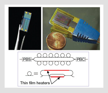 Components made with the Hydex platform. (Left) Photograph of a triplexer WDM chip. (Right) photograph of a packaged 16-channel tracking-demultiplexer based on microring resonators. (Bottom) A dynamic optical dispersion compensator circuit. PBS and PBC are polarization beam splitter and combiner. The dispersive elements are ring resonators having free spectral range of 50 GHz. The full physical circuit, including PBS and PBC, resides on a PLC chip measuring 9 mm x 11 mm.
Planar lightwave circuits
One can gain significant signal advantages by incorporating passive optical elements for switching, routing, filtering, multiplexing and power leveling onto an integrated chip. The primary function of such chips is to passively route and process incoming optical signals, so that they may be made with materials other than InP. The use of silicon chips allows for leverage of existing substrates, processing tools, fabrication processes and manufacturing knowledge from the microprocessor industry. Silicon-based integrated optical chips are known as planar lightwave circuits (PLCs).
To realize Si PLCs, a waveguide core layer is required that has a refractive index larger than the surrounding cladding layer. The index contrast between waveguide core and cladding determines the minimum bend radius for the waveguides and sets the waveguide dimensions for single mode performance. A high index contrast keeps the devices small and allows for efficient integration of many elements on one PLC. However, too high an index contrast will lead to tiny waveguide sizes that are more sensitive to process variability (i.e., critical dimension control), making efficient fiber coupling more difficult. As an example, Infinera’s novel PLC material system is based on a proprietary glass-based Hydex platform that uses conventional commercial silicon processing technology, and has an adjustable index contrast of up to 20 percent.
The process results in waveguide dimensions of approximately 1.5 µm x 1.5 µm and a bend radius of 35 µm. These dimensions enable a dramatic leap in component integration density. Integrated PLC chips can now be designed with a footprint of roughly 100 mm2, and hundreds to thousands of devices can be fabricated onto Si wafers that are 4 to 8 in. in diameter. An important aspect of this platform is that it exhibits low loss throughout the optical transmission window (< 0.16 dB/cm over 1,530-1,630 nm); this is a critical prerequisite for making high-performance, low-loss PLCs for telecom applications.
On this platform, compact mode transformers have been designed to enable efficient coupling to optical fibers. Furthermore, there are now manufacturing processes that are compatible with thin film heaters. These heaters can be used for phase adjustments and active electronic control of the optical elements by means of thermally tuning the local refractive index.
Engineers can now realize many fundamental optical processing components, such as filters, beamsplitters, interferometers, (de)multiplexers, polarization controlling elements, attenuators, etc. These components can be integrated into complex, large-scale PLCs, and they exhibit improved footprint, functionality, performance, cost and reliability compared with their corresponding bulk components. Researchers have demonstrated a wide variety of devices to date, including AWGs, tunable bandwidth micro-ring resonator filters, tunable optical dispersion compensators, triplexer filters and ring-resonator-based spectrometers.
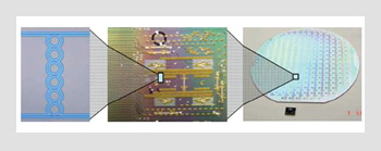 Ring resonator based PLC chip. (Left) Compound ring resonator. (Center) PLC chip with dense functionality. (Right) A silicon wafer with hundreds of PLC chips.
The figure on the right shows how elementary building blocks like the microring resonators are assembled to form large functional chips in the PLC platform. These chips are then fabricated by the hundreds to cover a large Si wafer and individually packaged. For example, commercially available 16-channel demultiplexers are larger than PLC devices by more than a factor of 10. These devices also eliminate multiple, manually assembled fiber splices between discrete components in complex, multi-channel systems, leading to improvements in component reliability and reductions in cost.
Clearly, the Si-based PLC technology holds great promise for further density scaling. PLCs are expected to find more applications within optical networks, reducing cost and complexity while improving the flexibility and reliability of optical telecom systems.
A new era of optical integration has arrived, and it is one that will provide improvements in capacity, speed, density and reliability concurrent with reductions in cost and power consumption. We have a solid foundation for optical network growth for decades to come.
The authors are with Infinera Corp. in Sunnyvale, Calif., U.S.A. Jacco L. Pleumeekers is a manager in the PIC integration engineering department. Peter W. Evans is a member of the technical staff for PIC development. Wei Chen is a member of the technical staff for PLC development. Richard P. Schneider Jr. is a senior director of PIC platform engineering. Radha Nagarajan is a senior director of optical component technology.
References and Resources
>> S.E. Miller. Bell Syst. Tech. J. 48, 2059–69, 1969.
>> Y. Kawamura et al. J. Quant. Elec. QE-23, 915-8 (1987).
>> M. K. Smit. Electron. Lett. 24(7), 385–6 (1988).
>> H. Soda et al. Electron. Lett. 26, 9-10 (1990).
>> H. Takahashi et al. Electron. Lett. 26(2), 87–8 (1990).
>> M. Aoki et al. Electron. Lett. 27, 2138-40 (1991).
>> C. Dragone. IEEE Photon. Technol. Lett. 3, 812–15 (1991).
>> T.L. Koch and U. Koren. IEEE J. Quant. Electron. 27, 641-53 (1991).
>> B. Mason et al. IEEE Photon. Tech. Lett. 11, 638-40 (1999).
>> C.G.P. Herben et al. Photon. Technol. Lett. 11(12), 1599 (1999).
>> Y.A. Akulova et al. IEEE J. Sel. Top. Quant. 8(6), (2002).
>> Y. Suzaki et al. IPRM (Sweden), 681 (2002).
>> Y. Yoshikuni. J. Sel. Top. Quantum Electron. 8(6), 1102 (2002).
>> M.L. Masanovic et al. Photon. Technol. Lett. 15(8), 1117 (2003).
>> B.E. Little. Proc. Optical Fiber Communications Conf. 2, 444-5 (2003).
>> R. Nagarajan et al. IEEE J. Select. Topics Quantum Electron. 11(1), 50-65 (2005).
>> Y.-H. Kuo et al. Nature 437, 1334-6 (2005).
>> A.J. Ward et al. IEEE J. Sel. Top. Quant. 11(1), (2005).
>> H. Rong et al. Nature 433, 725-8 (2005).
>> W. Chen et al. Proc. Optical Fiber Communication Conf. 2006, paper PDP12.
>> R. Nagarajan et al. IEE Electron. Lett. 42(13), 771-3 (2006).
>> D.F. Welch et al. IEEE J. Lightwave Technol. 24(12), 4674–83 (2006).
>> Z. Zhu et al. Proc. CLEO/QELS Conf. 2006, paper CThS5.
>> D.F. Welch et al. IEEE J. Sel. Topics Quantum Electron. 13(1), 22–31 (2007).
>> W. Chen et al. Proc. ECOC Conf. (2007).
>> W. Chen. “Integrated Polarimeter Assisted Ring Scanning Spectrometer,” Proc. ECOC Conf. 2008, paper P.2.17.
>> B. Little. Proc. ECOC Conf. 2008, paper Th.2.C.2.
>> D. van den Borne et al. Proc. Optical Fiber Communication Conf. 2008, paper OMQ1.
>> J.E. Roth et al. Electronics Lett. 44(1), 49-50 (2008).
