
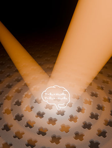
An artistic representation of the new optical development process, which speeds up design of devices by supplementing machine learning with equations representing the physical processes in play. [Image: Chalmers University of Technology, Viktor Lilja]
Scientists in Sweden have combined machine learning and physics calculations to design photonics components more quickly than is possible with either approach in isolation (Laser Photonics Rev., doi: 10.1002/lpor.202502769). They demonstrated their new method, which relies on accurately reproducing light scattering, in the design of both photonic-crystal slabs and devices made from free-form metasurfaces.
Designing with neural networks
Researchers traditionally design advanced optical devices using computer simulations based on Maxwell’s equations of electromagnetism. They do so by simulating the output of an initial random or obvious design, then work backward by using the difference between the simulated and desired output to tweak the design in the hope of improving it. Carrying out this process over many iterations eventually leads to a high-performance device.
Since the many simulation steps take a long time to carry out, numerous groups have instead turned to neural networks for optical design. The idea here is to train a network to, in effect, learn the physics underpinning the operation of the device in question. The network is fed many different designs at its input, with the weights of its neurons tweaked after each round in order to bring its output—parameters defining the device's optical performance—in line with the expected result in each case.
Such networks are usually able to calculate the output of a given design far more quickly than conventional simulations. In principle, they can also save lots of time when it comes to generating new designs, given that each step of the “inverse design” process is much shorter. However, design performance is limited by the accuracy of the neural network. That accuracy can be improved by increasing the number of parameters in the network or adding additional rounds to the training process, but doing so requires significant computing power to generate the extra data samples and can end up taking longer overall than conventional simulation when it comes to one-off designs.
Back to physics
Rather than using a neural network to directly work out the scattering matrix, the researchers instead trained a network to generate a series of parameters describing the quasinormal modes.
In the latest work, Philippe Tassin and colleagues at Chalmers University of Technology have shown how pure machine learning can be improved upon by inserting some physics back into the design process. They define the performance of devices by what is known as a scattering matrix, which relates the amplitudes of incoming and outgoing electromagnetic modes, revealing how much light is transmitted, reflected or absorbed. More specifically, they break the scattering matrix down into “quasinormal modes,” which define the decaying resonant frequencies of a physical system that loses energy.
Rather than using a neural network to directly work out the scattering matrix, the researchers instead trained a network to generate a series of parameters describing the quasinormal modes. They then plugged these values into an algorithm to calculate the scattering matrix. Doing so, they expected to reduce the amount of data needed to train the network, which they dubbed QNM-Net, while also ensuring that the system’s output designs conserve energy and obey the principle of causality.
Testing the scheme
They put their scheme to the test by getting it to design photonic crystal slabs, which consist of a sheet of lossless dielectric material patterned with an array of micrometer-sized holes. They started by training QNM-Net with 8,000 data samples—each comprising a random slab design and its associated scattering spectrum—before using another 2,000 samples to test the system’s accuracy. They compared these results with those from three standard fully connected neural networks (without a physics algorithm), finding that QNM-Net can achieve a given spectral accuracy with just a tenth of the data needed to train its more conventional counterparts.
The researchers then used the trained QNM-Net to carry out the inverse design of five different photonic crystal slabs. They were able to do so in less than one second per design, finding in each case that a computer simulation of the device’s output closely matched the output sought at the beginning of the exercise.
Tassin and colleagues also used QNM-Net to simulate the workings of more complex devices in the shape of free-form all-dielectric metasurfaces. Here they achieved about a three-fold reduction in the amount of training data needed to achieve a given loss compared with the best standard neural networks, but they failed in some cases to reproduce simulated scattering resonances—the design space being so large, they say, that not even the tens of thousands of data sets they used for training were enough to maintain high accuracy.
They point out that they are not the first group to integrate physics calculations into machine learning for the design of optical components. The researchers say that QNM-Net has a similar accuracy and training requirements to previous physics-enhanced neural networks, but they argue that their method could be used to design a wider range of photonic devices and has a more solid theoretical basis. Among the devices that could be designed by QNM-Net, they say, are lighter, better-performing lenses for cameras or glasses as well as perhaps photonic crystals for transmitting data between quantum computers.
