
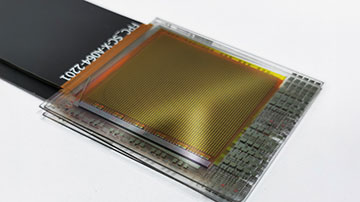
Researchers in Switzerland have built and tested two prototype thin-film image sensors, one of which is shown here, using vertically stacked layers of perovskite crystal. [Image: Empa / ETH Zurich]
Scientists in Switzerland have built a new kind of color image sensor that harnesses nearly twice as much incoming light as existing devices, thanks to pixels made from vertically stacked perovskite crystals (Nature, doi: 10.1038/s41586-025-09062-3). They say that if successfully scaled up, the technology could yield compact imagers with unprecedented resolution and color fidelity.
Challenges with silicon
Most digital cameras use silicon as the semiconductor to convert incident light into electrical current, but they are limited by the fact that silicon operates with nearly uniform efficiency across a broad range of wavelengths. Color images are produced via horizontally arranged filters, each one transmitting one of three colors from the visible-light spectrum—red, green or blue—while blocking the other two. This arrangement wastes most of the incoming light and limits the device's resolution.
In 2002, researchers at Sigma Corporation in Japan showed how to do away with filters by instead exploiting the fact that light penetrates to different depths in silicon depending on its wavelength. Their “Foveon” imagers consist of three vertical layers, each designed to absorb a different color—blue first, then green and finally red. However, the overlap in absorption bands distorts the device's color while larger-than-normal pixels limit resolution.
Light-absorbing crystals
In the latest work, Maksym Kovalenko and colleagues at ETH Zurich and the Swiss Federal Laboratories for Materials Science and Technology instead turn to crystals known as lead halide perovskites. These semiconductors convert light into electricity very efficiently, and they have absorption characteristics that can be tuned by altering their precise chemical makeup. The idea is to arrange three different perovskite crystals on top of one another, so that each layer absorbs just one of the three bands of light while allowing the others to pass through to the layers below.
The researchers demonstrated this principle several years ago using individual oversized pixels containing millimeter-sized crystals. They have now built two fully functional image sensors comprising thin films of lead halide perovskite doped with iodine ions to absorb red light, bromine ions for green light and chlorine for blue light.
Illuminating one of the prototype photo detectors from above, they measured its external quantum efficiency—the fraction of incoming photons that generate an electron—to be 53% for blue light, 50% for red and 47% for green. These figures are nearly double those of standard silicon sensors with filters.
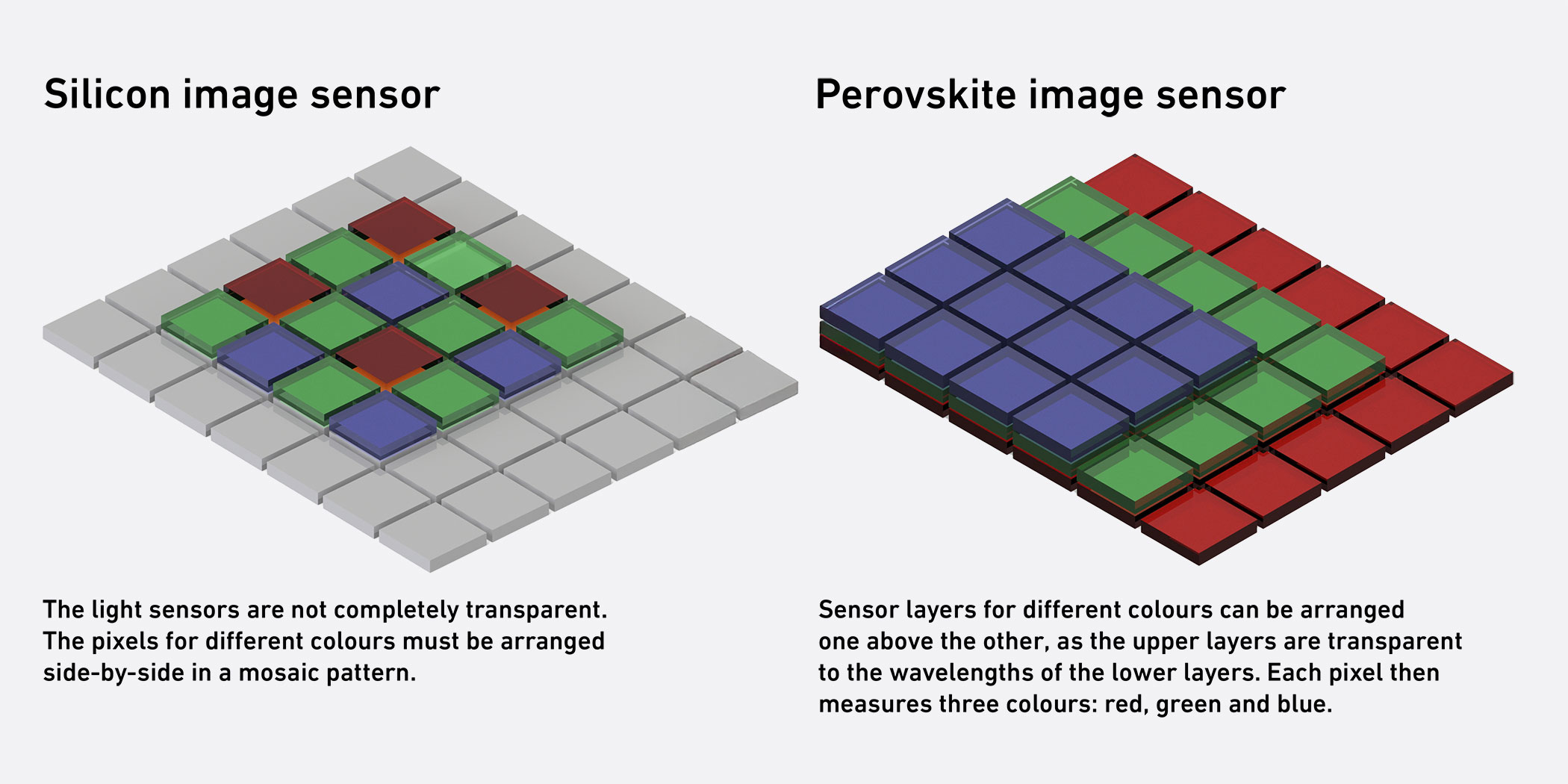
Comparison of a silicon image sensor and a perovskite image sensor. [Image: Sergii Yakunin / ETH Zurich / Empa]
The researchers also found that their device can better reproduce colors than existing sensors, finding the difference between displayed and original colors to be less than 4% on average. What's more, by building an array of 8×8×3 stacked photodetectors, they demonstrated that they could avoid the processing usually needed to overcome “demosaicing”—the interpolation of the missing colors in each (monochrome) pixel by analyzing the colors measured by adjacent pixels, which itself can reduce resolution and introduce color artifacts.
Kovalenko and colleagues reckon that by increasing resolution and using more of the incoming light, their sensors could become smaller than today’s devices, which they say could in turn reduce the size and complexity of consumer digital cameras. They also argue that the ability to precisely tune a perovskite crystal’s absorption spectrum could make the technology ideal for hyperspectral imaging, with potential applications in medical analysis and environmental monitoring.
Hurdles to overcome
Writing a Nature news and views commentary piece, Shuming Nie and Viktor Gruev at the University of Illinois at Urbana Champaign, USA, applaud the “striking” results from the new research. But they caution that many hurdles must still be overcome before such sensors can be commercialized. These, they say, include building pixel arrays larger than just a few millimeters across, ensuring that the perovskites employed remain stable when exposed to air or water and identifying crystals that don't contain (toxic) lead.
They also note that wiring the perovskite stacks to silicon readout chips will not be easy. The chips will have to handle three outputs from each pixel rather than one, while new architectures for stacked electronics will be needed to maintain high resolutions over centimeter-scale sensing areas. But, they argue, the reward for overcoming these problems “could be substantial.”
