
Crystal structure of the transition-metal dichalcogenide (TMD) molybdenum disulfide (MoS2). A research team at the University of Pennsylvania, USA, has modeled the potential of such 2D materials for applications, such as space-based power production, where light weight is a key parameter. [Image: B. Mills/Wikimedia Commons] [Enlarge image]
Silicon’s abundance and proven mass-production scalability have made silicon-based photovoltaics (PVs) the dominant solar-energy technology in Earth-based electricity grids. But commercial silicon solar cells are too heavy for a range of niche applications—including potential “utility-scale” energy production for long-term space exploration and settlements. That has spurred a search for alternative, thin-film materials, such as organic PVs and perovskites, that are lightweight enough to shine in such space-based applications, as well as in other weight-sensitive areas such as wearable tech.
A particularly intriguing possibility lies in so-called transition-metal dichalcogenides (TMDs)—inorganic, molecule-thin sheets with a range of favorable optoelectronic properties (see “Optoelectronics in Flatland,” OPN, July/August 2015). These super-compact materials have the potential to radically reduce the weight of solar cells for space-based applications. But while modeling has suggested that TMD-based PVs could in principle reach a power-conversion efficiency (PCE) comparable to that of crystalline silicon, actual experiments with TMDs haven’t come anywhere near silicon’s lofty efficiency numbers.
A research team led by Deep Jariwala at the University of Pennsylvania (UPenn), USA, has now dug into the relevant electronic and optical physics to suss out just why experiment hasn’t matched theory for TMD-based PVs (Device, doi: 10.1016/j.device.2023.100003). The work revealed that the practical PCE maximum for TMD devices is likely far lower than what’s previously been assumed. But the team also says that, by optimizing such devices in a “superlattice” design, TMD-based PVs could excel in another key parameter: “specific power,” or watts per gram.
That’s much more important than absolute PCE, Jariwala argues, when looking at utility-scale power production in space. “The weight of 2D [TMD] solar cells is 100 times less than silicon or gallium arsenide solar cells,” he said in a press release accompanying the research. “So suddenly these cells become a very appealing technology.”
Molecule-thin layers
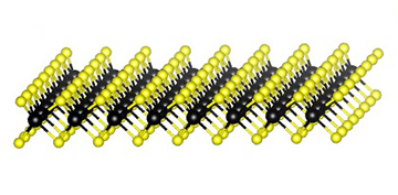
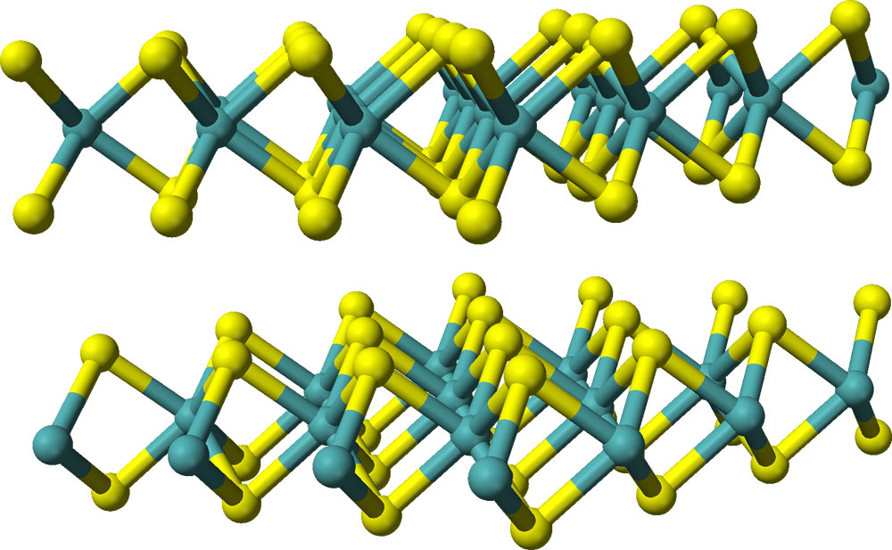
The “MX2” structure of TMDs consists of a transition metal, such as molybdenum or tungsten (black) between two layers of a chalcogen such as sulfur or selenium (yellow). [Image: 3113lan / Wikimedia Commons; CC-BY SA 3.0]
TMDs are so-called 2D materials, analogous to graphene. But instead of atom-thin sheets of carbon, TMDs consist of molecule-thin layers including—as their name implies—a sheet of atoms of a transition metal such as molybdenum (Mo) or tungsten (W), sandwiched between two sheets of chalcogen atoms such as sulfur (S) or selenium (Se).
A particularly intriguing feature of TMDs lies in their band structure. These materials have only an indirect band gap as bulk crystals. But when they’re thinned down to monolayers, the quantum confinement causes the structure to change to a direct band gap.
That band-gap transition opens the prospect for building photodetectors, solar cells, LEDs and other optoelectronic devices from 2D TMDs. And indeed, calculations under the so-called detailed balance model—a widely employed, simplified model for calculating the maximum theoretical efficiency of a PV device—suggest that TMD-based PVs can achieve PCEs on the order of 27%.
Such efficiency levels would put TMD-based PVs close to lab-demonstrated efficiencies for silicon-based solar cells. But, according to the UPenn team, experimental PCEs typically reported for TMD devices have come in far lower—at 2% or less. And even in the best lab results, TMDs have rarely achieved PCEs better than around 6%.
The exciton factor
Jariwala’s team wanted to find out why experimental efficiencies have fallen so short of the modeling—and to see if a better design for TMD-based PVs could move the needle higher. To do so, the researchers took a deep dive into the physics of excitons in these 2D materials.
The team wanted to find out why experimental efficiencies have fallen so short of the modeling—and to see if a better design could move the needle higher.
Excitons are “quasiparticles” formed when a solar photon strikes the PV material and excites an electron, kicking it into the conduction band and leaving behind a so-called electron hole. The exciton is the bound state connecting the excited electron and the hole. The authors of the new study write that, while excitons “dominate the optical response” of semiconducting 2D TMDs, attempts thus far to determine how well TMD-based PVs can theoretically perform “have failed to treat excitons seriously.”
The UPenn scientists attempted to remedy that shortfall, drilling down into exciton binding energy, diffusion length, and radiative and nonradiative lifetime, as well as carrier mobility and the effect of incidence angle on photocarrier generation. To test out how varying those parameters would affect both PCE and specific power, they plugged them into a model of a previously reported “superlattice” structure. The structure in question consisted of up to 10 separate monolayers of the TMD MoS2, separated by insulating layers of Al2O3, all atop a reflective gold layer to facilitate the bouncing of light among the active layers in the solar cell.
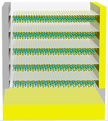
The superlattice design explored by the UPenn team consists of multiple active layers of the TMD MoS2 (yellow and green), separated by insulating layers of Al2O3, atop a reflective gold layer, and configured between silver (left) and gold (right) electrodes. [Image: Device / Hu et al.]
PCE versus power density
The team found that even the best case—a five-layer superlattice structure, with optimized geometric and material properties—would achieve maximum PCEs of only around 9.2% to 12.9%, depending on details of the electrode configuration. That’s well ahead of most experimental results for TMD-based PVs thus far, but far below the 27% theoretical maximum efficiency predicted from the simpler detailed balance model. The authors tie that discrepancy to the fact that the latter model assumes perfect spectral absorption that isn’t matched in the UPenn team’s more realistic optimized simulation.
All is not lost for TMD-based PVs, however, especially for applications in which weight is a key piece of the puzzle. The UPenn researchers’ calculations indicate that while PCE levels don’t approach those of state-of-the-art PVs, the power density, or specific power, for its optimized designs are between 157 W/g and 220 W/g, owing to the extremely small, 3.5-nm thickness of the active layer. That’s a better power-per-weight performance, the team says, not only than conventional solar-cell materials such as silicon and gallium arsenide, but also compared with other emerging lightweight materials such as perovskites and organic PVs.
Such a high specific power, Jariwala said in the press release, is “one of the greatest goals” of space-based energy harvesting, and essential for “real utility-scaled power in space” as well as for other mobile applications. There’s still work to be done, though, in getting to wafer-scale production of the team’s superlattice design—the issue that Jariwala’s team will be tackling next.
