
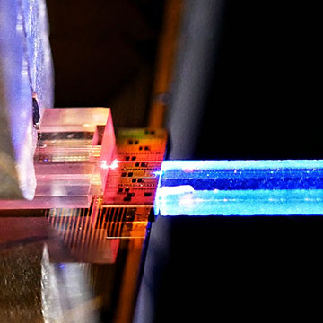
Researchers have shown how to hook up a nonlinear crystal and photonic integrated circuit to create pairs of photons at visible and telecom wavelengths, enabling heralding of the telecom photon via a fairly simple room-temperature visible detector. [Image: RIT]
Researchers in the United States have built a compact source of single photons at telecom wavelengths that might in future be used to make the nodes in a quantum network (Opt. Quantum, doi: 10.1364/OPTICAQ.546774). By generating each photon alongside a visible counterpart, the device allows heralding via fairly compact detectors and could potentially hook up diverse quantum computers over long distances.
Toward a smaller source
Quantum-encoded light is already used commercially to generate secret keys for encrypting classical data. But scientists also are looking to develop networks that transmit data between quantum-mechanical computers or sensors, in which matter-based quantum bits (qubits) within such devices are connected to one another via “flying” photonic qubits.
Like an ever-increasing fraction of today's internet, the links in such networks would likely be made from lengths of optical fiber. But detecting single photons with wavelengths that propagate most readily along such fibers—around 1550 nm—currently requires bulky superconducting detectors that operate at cryogenic temperatures.
Preble and colleagues have now shown how to combine the best of both worlds.
In the latest work, Stefan Preble, Vijay Sundaram and colleagues at the Rochester Institute of Technology and elsewhere show how smaller, room-temperature single-photon avalanche diodes (SPADs) can replace these devices thanks to the generation of pairs of photons—one photon at telecom wavelengths and the other in the visible region of the spectrum. The telecom photon would be used to carry quantum information, with its creation “heralded” by the detection of the visible photon at the SPAD (heralding being needed because single photons are generated at random points in time).
Such photon pairs can be readily produced inside certain crystals via a second-order nonlinear process known as spontaneous parametric down conversion. One such crystal is lithium niobate, which can also be fashioned into integrated circuits, potentially enabling single photons to be produced and manipulated on a single chip. Lithium niobate, however, is not compatible with the pre-existing multi-billion-dollar CMOS manufacturing infrastructure. On the other hand, CMOS-compatible silicon exhibits much weaker third-order nonlinearities.
Best of both worlds
Preble and colleagues have now shown how to combine the best of both worlds. They “edge-coupled” waveguides on a 1.5-cm-long nonlinear crystal made from periodically poled potassium titanyl phosphate with others on a 4-mm-long photonic integrated circuit etched from two layers of silicon nitride and one of silicon. Both the crystal and circuit serve dual functions. The former generates photon pairs and splits them up by incorporating a wavelength division multiplexer. The latter manipulates the telecom photons via a thermally tuneable Mach–Zehnder interferometer, while also filtering out the intense blue light generated by the pump source (the silicon waveguide strongly absorbing such light).
The researchers sought to establish how reliably the visible photons would herald the arrival of their telecom counterparts after sending the former straight through the integrated circuit while encoding the latter using the interferometer. They defined success as the detection of a visible and telecom photon within 1 nanosecond of each other and initially used bulky superconducting detectors to register each photon in a pair. Doing so, they recorded a little over 11,000 successes per second. When the team switched to a SPAD for the visible photons, the performance level dropped to just under 10,000 coincidences a second.
Real-world application
Despite this drop, the researchers are confident they can deploy their system in the field and demonstrate the virtue of fairly small, cheap SPADs for setting up remote nodes in a quantum network.
Preble and coworkers also gave a flavor of what could be achieved in a real-world network by connecting the telecom photons' output port to two 19-km-long sections of dark optical fiber—one sending the photons from the Rochester Institute of Technology to the University of Rochester and the other sending them back again. Loss, however, caused a sharp drop in performance, leading to no more than about 30 coincidences per second, even with a “coincidence window” extended to 10 ns.
Despite this drop, the researchers are confident they can deploy their system in the field and demonstrate the virtue of fairly small, cheap SPADs for setting up remote nodes in a quantum network. But first, they say they need to better couple telecom photons to their system, perhaps by using dedicated edge couplers and also optimizing their chip fabrication. They also plan to better package circuit, crystal and pump together in order to maintain high coupling levels over extended periods.
Looking further into the future, the team points out that incorporating multiple poled regions within their nonlinear crystal would allow the system to generate highly entangled states of visible-telecom photon pairs for carrying out quantum teleportation between distant quantum nodes, “advancing the field of heterogeneous quantum networking.”
