
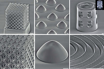
A team at Karlsruhe Institute of Technology, the University of California Irvine, and Edwards Lifesciences has developed a method to 3D-print glass micro- and nanostructures, such as (left to right) the nanolattice, parabolic microlenses and multilens micro-objective shown here, at temperatures far lower and resolutions far higher than with previous glass-nanoprinting schemes. Scale bars: 10 µm. [Image: Reprinted with permission from J. Bauer et al., Science 380, 960 (2023); doi: 10.1126/science.abq3037]
The 3D-printing process called two-photon polymerization (TPP)—also known as direct laser writing—has enabled some spectacular and intricate nanoscale structures. But to date, much of the technique’s magic has been performed in plastic, using specialized, printing-friendly polymer resins.
Optical scientists and engineers would love to use TPP’s flexibility to create freeform nanoscale structures in that most time-tested of optical materials, silica glass. But while some glass-nanoprinting schemes have emerged from research labs, they commonly have required sintering of silica nanoparticles at temperatures of more than 1100 °C. That’s far too toasty to be useful in a range of important applications, such as direct deposition on semiconductor chips. What’s more, such sintering-based processes result in features with insufficient resolution for visible-light applications.
Now, a research team led by Jens Bauer at the Karlsruhe Institute of Technology (KIT), Germany, reportedly has developed a different approach for 3D nanoprinting of very-high-quality, high-resolution optical glass—one that slashes the required processing temperatures by some 500 °C (Science, doi: 10.1126/science.abq3037). The lower temperature opens the prospect of 3D-printing tough, transparent and freeform glass optical structures directly on semiconductor chips, at the resolutions required for visible-light nanophotonics.
“What we achieve with this,” Bauer told OPN, “is that we really are able to make this high-quality, inorganic glass with the same level of printability and ease of use that people who use TPP know from commercial, standard polymer resins.”
The quest for nanoprinted optical glass
The nonlinear process of TPP works by exposing a photoactive resin, chemically tuned to crosslink into polymer chains on simultaneous two-photon absorption, to tightly focused femtosecond laser pulses. The system allows the creation of solid structures at micrometer and even nanometer scales—and its flexibility has enabled the printing of freeform nanoscale optical structures directly on microchips. But those structures have generally been written in polymer, a material with highly variable optical and mechanical properties, and without the environmental stability and toughness of glass.
TPP printing’s flexibility has enabled printing of freeform nanoscale optical structures directly on microchips—but those structures have generally been written in polymers, not glass.
Efforts to extend the flexibility of TPP printing to nanoscale optical-glass structures have generally relied on “particle-loaded” polymer binder resins as the raw material. As the name implies, these binders include nanoparticles of silica suspended in a photocurable resin. On laser exposure and two-photon absorption, the resin binder polymerizes and crosslinks the silica nanoparticles. The crosslinked particles are then fused together into glass in a final sintering step—at temperatures on the order of 1100–1300 °C—that also drives off the polymer binder.
The sintering system unquestionably can fashion some exquisite 3D-printed glass microstructures. But the required temperatures lie above the melting points of key semiconductor materials such as germanium and indium phosphide—not to mention those of most metals that are important in electronic circuits. That means that TPP printing that relies on particle-loaded resins is impractical for direct on-chip fabrication of nanoscale optical glass.
Further, the finite size of the particles being sintered together imposes minimum feature dimensions (as well as an inherent surface roughness) that limit the printing resolution. That’s a drawback, as the resolution of structures 3D-printed using particle-loaded binders tends to be a hair too coarse for applications in visible wavelengths.
Chemistry lesson
To get around these drawbacks, Bauer, along with colleagues at the University of California Irvine and Edwards Lifesciences, Irvine, CA, USA, focused on the resin chemistry. Rather than using a suspension of silica nanoparticles, the team developed a recipe for a liquid resin built around so-called polyhedral oligomeric silsesquioxane (POSS) molecules. These are hybrid organic-inorganic molecules that include tiny cagelike silica molecules, decorated with organic functional groups to create a monomer structure.
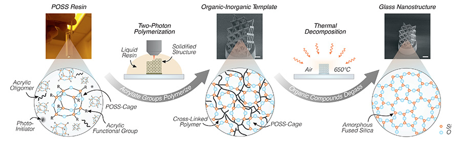
Schematic view of process, from synthesis of POSS molecules (left) through TPP printing (center) to final themal-treatment step at 650 °C (right). [Image: Reprinted with permission from J. Bauer et al., Science 380, 960 (2023); doi: 10.1126/science.abq3037] [Enlarge image]
To fashion its POSS monomer, the team functionalized the inorganic molecular cages with organic acrylic groups at the corners, to allow crosslinking of the silica cages in a close-knit, continuous network. They added a photoinitator to the POSS resin, to kick off crosslinking of the monomers on two-photon exposure. And the team’s recipe also spikes the resin with highly flexible, free-floating acrylic oligomers. This last ingredient, says Bauer, further facilitates crosslinking, and “allowed us to achieve very high print quality,” despite working with “rather rigid POSS molecules that don’t like to crosslink that easily.”
Finally, once the fully 3D-printed, crosslinked nanostructure is formed, it is heated in air to a temperature of 650 °C. This last step drives off the organic components and completes the linking of the inorganic POSS silica cages, to form a continuous glass micro- or nanostructure.
The required temperature is half of what’s needed for approaches that rely on sintering of nanoparticles. That, Bauer said, is because the individual silica clusters are very small—“only a handful of atoms.” The TPP process packs those molecular clusters very close together, keeping the required fusing temperatures far lower than what’s required for the sintering of (comparatively huge) silica particles.
Toward on-chip, freeform glass nanoprinting
Bauer and his colleagues used their POSS resin to TPP-print a variety of nanoscale optical structures—including “woodpile” photonic crystals with 97-nm free-standing features, arrays of parabolic microlenses, and a multilens micro-objective including nanostructured Fresnel elements. The flexibility afforded by TPP printing also enabled the researchers to build freeform glass micro-optics that show “excellent optical performance,” according to the paper, and that have minimum feature sizes and surface roughness small enough to enable visible-light nanophotonic devices.
“This really paves the way to on-chip manufacturing,” Bauer told OPN.
The researchers write that their lower-temperature system “brings the freeform synthesis of silica glass below the melting points of essential materials for microsystems technology,” and thereby “represents a breakthrough that enables the evolution of on-chip 3D-printing of transparent matter” to include “resilient optical-grade fused silica.” Bauer told OPN that he believes the system has “a broad range of micro-optical and photonic applications”—particularly for systems that might face harsh chemical, thermal or other environments where 3D-printed polymer structures might not hold up.
“This really paves the way to on-chip manufacturing,” Bauer told OPN. “For pretty much any chip that can sustain 650 °C, it will be possible to print high-quality, clear glass micro- and nanostructures directly on the chip.”
