
![]()
Christian Reimer. [Image: Courtesy of C. Reimer]
The July/August 2023 issue of Optics & Photonics News featured the magazine’s biennial feature spotlighting 10 Entrepreneurs to Watch. Here, we offer an interview with one of those entrepreneurs, Christian Reimer, a cofounder of HyperLight, a spinout from Harvard University, USA, that specializes in thin-film lithium niobate integrated photonics. Reimer serves as the company’s Head of Product.
What is HyperLight, the company you cofounded, trying to do?
Christian Reimer: Everybody at HyperLight really believes in the power of integrated photonics—it has, in our mind, a massive promise and could have a significant impact on society in many applications. But silicon photonics and integrated photonics have not yet scaled as have silicon electronics or microelectronics.
So the goal, what drives us, is that we want to maximize the potential of integrated photonics, essentially to proliferate it and make it at the scale of electronics. And when we talk about scaling, we don’t mean scaling it like Moore’s law … we are talking about the social impact, the economics.
To do that, we think we need to combine the best performance, stability and versatility with making it producible at cost and at scale. And we believe that silicon, even though it’s amazing for electronics, is actually not the best platform for photonics.
And thin-film lithium niobate is the right platform?
The unique thing about thin-film lithium niobate is that it provides exceptionally good performance. It’s the only platform that I know of that can address, at the same time, market segments that are driven by ultra-high performance, as well as high-volume markets that are driven by cost.
“Everybody at HyperLight really believes in the power of integrated photonics—it has, in our mind, a massive promise.”—Christian Reimer
I think this combination allows lithium niobate to become one of the leading platforms that can make use of all the aspects that integrated photonics can offer. And HyperLight’s mission is to enable that.
We purposefully decided to focus on photonic chip solutions—we design them, we push the technology, we build the infrastructure—because there hasn’t really been a volume-ready, mass-producible vehicle to bring thin-film lithium niobate to scale. And we cooperate very deeply with our customers, who actually represent many different market segments.
That is, I believe, the key for us—focusing on delivering the best photonic chip solutions to our customers.
Maybe a little bit more on lithium niobate—what makes it such an interesting material, and gives it these better performance characteristics?
Because it is naturally electro-optic. If you look at where silicon photonics or photonics in general is being used, it’s mainly driven by modulators—transferring electrical signal into optical signals. And the cleanest, fastest way to do that is to use the Pockels effect—the natural material electro-optic effect. You apply a voltage; you change your refractive index.
That is incredibly fast. And lithium niobate is one of the best materials that have that. Interestingly, it doesn’t have the highest electro-optic coefficient. But if you look at the electro-optic coefficient and the dielectric constant, which kind of means how much electric field you can get in there, it’s very, very good.
It’s also fully proven. It’s a stable material and it can be cheap … it’s very mature. And it has these amazing optical properties, like very low loss and this high electro-optic coefficient. And a reasonably high refractive index, to make it compact. That’s also important—that you can confine the modes tightly.

[Image: HyperLight Corp.]
And if you compare that, for example, with silicon or indium phosphide, silicon doesn’t have an electro-optic coefficient. It’s a centrosymmetric crystal. So you have to play tricks with the material and be clever, to get it to be electro-optic. You can do that by doping, but once you dope … you’re limited by the carrier mobility, and you’re adding extra losses. The losses in a silicon modulator are in the order of 5 dB; the losses in lithium niobate can be around 1 dB on a whole chip. That’s a massive difference.
Indium phosphide is very fast, but for modulation, people are mainly relying on other effects that … basically shift the bandgap. That can make it very sensitive to wavelength and temperature. And there are not that many people that can make indium phosphide at sufficiently high quality and adequate yield, because you have to grow quantum wells and heterostructures, and it’s very complicated.
So lithium niobate checks all of those boxes—performance and simplicity?
Yes. The power of lithium niobate is that once you figure out how you can make a thin film and etch it to define your structures—and we have figured that out—it is amazing how simple and elegant the devices can be. In very simplified terms, all you have to do is put electrodes next to a waveguide and the natural properties of lithium niobate turn it into a modulator.
So the biggest question that we addressed over the past several years was not to prove that lithium niobate is a good platform or good material. It was to prove that it could be made at volume, at scale, at cost and at yield. That was really our main focus.
And we now have ISO-qualified, high-volume production capabilities. We can ramp up from tens to hundreds to thousands or even millions of chips if the demand asks for it. And the amazing thing is that these chips, even at high volume, can provide exceptionally high performance.
“The power of lithium niobate is that once you figure out how you can make a thin film and etch it to define your structures … it is amazing how simple and elegant the devices can be.”—Christian Reimer
We just launched our first, 110-GHz packaged modulator. You know, applications like RF-over-fiber have been waiting for this for a long time—to have a low-loss, high-bandwidth, low-voltage modulator. And we can now address those at the same time, which makes me really excited.
When people talk about scalability in integrated photonics, they often are talking about something that plays well with the existing CMOS infrastructure. It sounds like the kind of volume production you’re talking is taking place in a separate system.
Let me try to elaborate a little bit.
I personally don’t think it is a good idea to actually have high-end electronics and optics on the exact same chip. Because, for the high-speed electronics, the latest technology is moving to 3-nm nodes. That’s incredibly expensive, and so to get to the price you need there, you need to get the volume really high up. You also usually want to use thin silicon and oxide in electronics; whereas for optics you want to have exactly the right thickness of silicon and box for mode confinement. And then your structures are limited by wavelength, so they are massive and don’t scale in the same way as electronics.
So you wouldn’t, in my mind, actually want to put high-performance electronics and optics on the same chip right now. You would probably still run silicon photonics on a different node, even though you’re utilizing the same tools [to make the chips].
And another issue is wafer size and volume—do you really need to run silicon photonics on 300-mm wafers? There was an interesting comment in the Rump Session at OFC 2023, which was something like, “if you took all of silicon photonics today, production would roughly equate to less than a week of wafer starts on one line at TSMC”. So the volume compared to electronics is simply not there (yet).
And this is where we purposefully designed our lithium niobate process flow. We chose the wafer size that made most sense to us, and utilized available, really good CMOS-style high quality equipment, running it through very established, stable lines—but running it in a way that scales correctly for photonics.
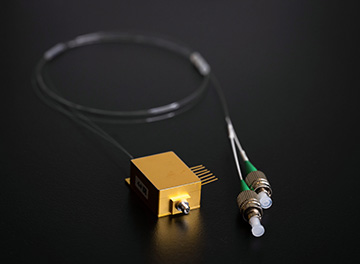
A HyperLight TFLN packaged electro-optic modulator. [Image: HyperLight Corp.]
So the volume we can do at the line that we already have is definitely enough, and future proof for telecom, datacom and other volume markets. And if the volume explodes, we can extend it and get more wafers in.
Let’s talk a little about you and your background, and the road you took to cofounding this company. When did you first become interested in science, and in optics and photonics in particular?
Well, I was always really into science, even in high school. My parents are both physics teachers, so that probably helped. And right out of high school, I went to Karlsruhe Institute of Technology (KIT), in Germany, to study physics.
In my second year, I think, I got to know solid-state physics, atomic and optical physics, and it fascinated me. I applied for a year abroad in Scotland, and did a master’s there in optoelectronics and lasers, with a focus on photonics, and I really, really loved it. I also got to know quantum optics; I worked on single-photon detection in the group of Gerald Buller, and learning new aspects of what a photon is or can be—by measuring clicks on a detector.
I really enjoyed my time in Scotland and met my wife there, so I decided to stay another year, going to the University of St. Andrews, in the group of Thomas Krauss … I did a second master’s there, learning about integrated photonics. And that also really fascinated me—that you can now, at the micro or nanometer scale, manipulate light to do things that you want it to do. So I chose to do a Ph.D. combining both—quantum optics and integrated photonics—at the National Lab in Canada in the group of Roberto Morandotti.
I think HyperLight was incubated in the lab of Marko Lončar at Harvard, in the US. How did you end up there?
Well, after earning my Ph.D., I met Marko at a conference in Boston, where I was giving a talk. He invited me to his lab to visit it. And after the visit, we met again at different conferences, and just kind of started talking. And when I was getting closer to graduation he offered me a postdoc position in his group, which was a dream come true for me.
I actually had a Marie Curie fellowship from the European Union. And the initial plan was to work on diamond photonics and quantum optics, because Marko is very active in that area and I wanted to stay in the quantum field. I envisioned myself becoming a professor and going into academia, which had been my dream since starting my Ph.D. studies.
But pretty much on the first day that I arrived in Boston, full of energy, I was sitting next to Mian Zhang, who’s a cofounder and CEO of HyperLight. And he showed me thin-film lithium niobate, and I was blown away. This was just before their big Nature paper. And I immediately fell in love with the material and got really excited about what it could mean for the entire field of integrated photonics.
And I got along really well with Mian—who is the main driver of HyperLight and TFLN technology as a whole. And we shared the same vision of what lithium niobate could do for the industry. So after just one year at Harvard, I canceled my Marie Curie fellowship, and became a cofounder of HyperLight, which was the best professional decision of my life.
Was there already talk of commercializing this when you arrived at Harvard?
Yes. When I got to Harvard, there was actually already a significant conversation around starting a company, and that was already in the works. So I was just in time to join the party. It was an interesting kind of “right place, right time” moment for me, and luckily I saw the potential, because I wasn’t really involved in developing the hard technology to that point.
“When I got to Harvard, there was actually already a significant conversation around starting a company … I was just in time to join the party.”—Christian Reimer
But from that point, I was very much involved with commercializing it, realizing the potential of HyperLight and helping to shape the company’s focus.
So after I had been at Harvard for just one year, we spun out HyperLight and got VC investment. And the last years have been an incredible journey.
You said you were envisioning yourself in academia. But before HyperLight, you also cofounded another company, KI3 Photonics. Can you talk about what you learned from that experience?
I think that was absolutely critical for me personally. So KI3 Photonics—the name the third-order chi nonlinearity—was initially about building mode-locked-laser or nonlinear sources, though at the end we actually changed a bit to stabilized interferometers and quantum applications. It was a very fun experience, founding it. And KI3 is still doing very well, but I am no longer involved in the business, though we keep in touch.
In fact, I think my biggest takeaway was that if you really want to start a company, I believe that you have to put all your efforts into it. I was doing a Ph.D., and I wasn’t willing to put all my efforts in [at KI3]. For me, it was a fun thing to do, to build a successful prototype and talk at conferences about it. But you know, it didn’t go anywhere while I was involved. Only more recently, after I left and the other cofounders are putting a lot of effort in it, is it taking off.
So the lesson is …
You either have to go all-in, or you don’t do it. That was also the key when I was talking to Mian about HyperLight—I said, “I don’t think you can do both; you can’t be a postdoc and try for faculty positions while building a company. I really believe in it, and I want to go all-in.” That’s why I canceled my fellowship. If I hadn’t had that, I probably wouldn’t have done HyperLight; I probably would have kept the Marie Curie and applied for faculty positions.
You could still have worked on lithium niobate.
“If you really want to start a company, I believe that you have to put all your efforts into it … You either have to go all-in, or you don’t do it.”—Christian Reimer
Yes—hypothetically, if I were to be a professor, I would for sure work on lithium niobate. And I would build the technology, and I would see how far we could push it. But my other thought was, if we can do that within the envelope of a company, we have the privilege to really focus and drive things like mass production.
As an example, if I had stayed in academia, I would have continued to use e-beam [fabrication], because it has the flexibility and the tools are there. If you go into a company, you are almost forced to address the core technology points. And that’s exactly what we did at HyperLight. The first years, we were mainly pushing to go from an individual chip with e-beam to wafers with UV lithography.
That was hard. But once we got there, suddenly our growth, in terms of what we could do with the technology, was exponential. We recognized from the beginning that a company is the better vehicle to do that.
Let’s talk a bit more about the process of spinning out HyperLight and selling the technology to investors. What were some of the big milestones there?
In addition to Mian and myself, a third cofounder who went full time is Kevin Luke, who had done his Ph.D. with Mian at Cornell University. Mian’s thinking was, if we bring one person in, it had to be Kevin, because Mian knew how good he is on the fab side, driving the wafer-scale production, and technology development in general. So there were three full-time people. And Marko is also a cofounder and advisor. A fifth founder, Cheng Wang, was a Ph.D. student in Marko’s lab who developed the technology together with Mian, but he chose to go into academia and is not actively involved in the company.
We were connected to various VCs through Harvard; this was really Mian going to a lot of VCs pitching the idea. And at the end of 2018, we got a term sheet and funding from a local VC called The Engine, which originated out of MIT, that focuses on “tough tech”; they do a lot with hardware, and their focus is on longer timelines. So they’re kind of funding 10- or 15-year timelines for product development in hardware technologies.
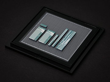
HyperLight is developing TFLN transmitter (Tx) PICs that, according to the company, can serve as “a simple drop-in replacement of existing silicon photonics or InP Tx solutions”—and achieve 40% power savings at the system level. [Image: HyperLight Corp.]
And that was a blessing. Because they provided us with office space, with an infrastructure where a lot of different companies were in the same building, and you could kind of soak in all the experience. They would organize workshops. It was all very, very helpful.
For the first few months, it was just the three of us full time. And we hired one Ph.D. from Marko’s lab, who’s an incredible asset and is still with the company, and another recent graduate from Yale. We really wanted to start scaling at that point—but then COVID hit. So we actually stayed just five people during the first year of COVID. And at the end of 2020 or the beginning of 2021, we started to hire more aggressively and really scale up.
Could you just describe a little bit more about your role at HyperLight vis-a-vis those of your cofounders?
Sure. My role is essentially product oriented. The main focus is, let’s take the technology we have or identify what we have to improve, talk to customers, identify their needs, and then work closely, build deep collaborations, and develop chips that work for them. It’s more on the immediate product side …
Kevin is the head of technology development. So he’s more driving on: Okay, what’s the future? Where can the technology go? Pushing the peak performance, implementing new functionalities. Still working with customers—we actually have a lot of customers that are willing to support R&D projects. But that’s on a longer time horizon.
And Mian is the CEO—he does everything. He’s the driving force that helps us to keep on track and push the direction.
Let’s talk now about where HyperLight has gotten to, in funding and in current and potential products. I believe you’ve logged a number of world records in this product space. How has the uptake been among clients, and where do things stand now?
We are very good in terms of the chip performance. Our customers are very happy; we have hit the milestones in terms of technical performance, especially for data comm and telecom customers.
I think the biggest breakthrough that really enabled us to address this, though, is that we figured out production. We can now produce thin-film lithium niobate in a fully ISO-qualified, fully scalable, high-volume production line. And that is really, really important. Because that helps us to look at yield and reliability, and make sure that we can deliver not just ten or a hundred great chips, but thousands or tens of thousands or hundreds of thousands.
“I think the biggest breakthrough … is that we figured out production … It’s not as colorful or flashy as us breaking a world record, but it’s the backbone that will enable TFLN make a real impact.”—Christian Reimer
That is, I think, one of our biggest breakthroughs. It’s not as colorful or flashy as us breaking a world record, but it’s the backbone that will enable TFLN make a real impact.
Looking at the entrepreneurial road you have walked thus far, what are some of the key lessons that you feel you’ve learned during this process?
I think it’s very important to talk to customers early and really learn what their pain points are. And not the pain points today, but what their pain points could be in a few years.
And then I think the second thing that I’ve noticed is that everything comes down to building trust, building relationship between people, and aligning goals. If you only talk to a sales team, their goal is to make a sale. But if you’re talking to a decision maker and align to the direction where they want to go, this can then become a fruitful, win-win collaboration. That’s something that I still put a lot of effort and time into—make sure to align everybody on the big picture, on the right direction, and then use that to drive the project.
How would you sum up HyperLight’s long-term vision, and where you and your cofounders want to take this?
The long-term vision is that we want to maximize the potential of integrated photonics. Essentially, we want to proliferate integrated photonics and make it at a scale comparable to silicon electronics—to build that infrastructure … We believe that by building a purposeful, truly high-performance platform for photonics, we can create an infrastructure that can drive new technologies, make an impact in terms power savings and new applications, and ultimately have a positive contribution to society and humankind.
That’s essentially the vision that drives HyperLight. And we believe that our platform and our approach will allow us to achieve that.
