
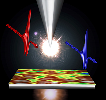
Visualization of the microscope tip exposing material to terahertz light. The colors on the material represent the light-scattering data, and the red and blue lines represent the terahertz waves. [Image: US Department of Energy Ames National Lab]
Terahertz radiation, with wavelengths that range from 1 to 0.1 mm, lies within the transition region between the microwave and far-infrared bands. Since the 1990s, the interest in terahertz radiation has continued to grow, with applications in information and communications technology, non-destructive sensing and imaging, and biology.
Now, scientists at the Ames National Laboratory, USA, have developed a terahertz microscope that uses a sharp metallic tip to probe complex materials with nanometer spatial precision (ACS Photonics, doi: 10.1021/acsphotonics.2c00861). The team used the microscope to image perovskite photovoltaic films; its findings, the group believes, may help optimize the power conversion efficiency and stability of future solar cells.
Applying terahertz light to perovskites
Jigang Wang and his colleagues built a terahertz system that relies on a technique called scattering-type scanning near-field optical microscopy (s-SNOM). Generally, s-SNOM offers a way to overcome the optical diffraction limit on the spatial resolution for surface spectroscopic analysis. It works by scanning a sharp, nanoscale-radius metallic tip over the sample with an atomic force microscope in tapping mode to enhance and probe the local electric field.
While the method has been applied to perovskite solar cells using infrared light, the current study is the first to apply terahertz s-SNOM to the promising photovoltaic material. Specifically, it aimed to investigate grain boundary defects in the crystal structure of a methylammonium lead halide perovskite (MAPbI3) thin film.
“The use of light or electromagnetic waves in the terahertz frequency band has been a relatively more recent development in the field, which we have also realized in our lab,” said Wang, study author and senior staff scientist at Ames National Laboratory. “We were interested if our new terahertz microscope could resolve the granular structures of perovskite materials.”
Visualizing grain boundary defects
Since their invention in 2009, perovskite solar cells have shown impressive device performance in terms of power conversion efficiency. However, problems with long-term stability remain a challenge for the technology, especially compared with the incumbent crystalline silicon solar cells, which boast a lifetime of roughly 25 years.
One key to improving perovskite stability is further exploring what happens during degradation in order to prevent or slow it down. In particular, grain boundary defect traps lead to nonradiative recombination and degradation centers, effectively limiting both stability and power conversion efficiency.
With their terahertz s-SNOM system, Wang and his colleagues could visualize the defect carrier traps in the granular surface of the MAPbI3 thin film at the single-grain-boundary level. They produced an image of the material degradation by tracking the local defect distribution over time. The results demonstrate higher carrier trapping at grain boundary defect ions compared with the grain interior, suggesting a distinct degradation pathway starting from grain boundaries that leads to defect propagation further in.
“Such findings can be used to understand the local charge transfer properties and improve [the performance] of these solar cell materials,” Wang said. “Better understanding of these issues may enable developing highly efficient perovskite-based photovoltaic devices for many years to come.”
