
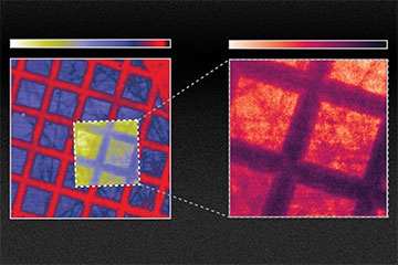
A measured X-ray image of a TEM grid on adhesive tape. The white-bordered square shows the area subject to photonic-crystal nanopatterning; the balance of image area is unpatterned. Scale bar shows strength of scintillation signal—maximum (white) to minimum (black)—indicating the increase in scintillation strength due to the nanopatterning. Right: Flat-field-corrected zoom-in of nanopatterned area. [Image: Courtesy of the researchers, edited by MIT News]
Scintillators form an integral part of many imaging and inspection systems, from electron microscopes to dental X-ray devices and night-vision equipment. The scintillation process depends on materials that can absorb high-energy photons or particles and convert their energy into light as efficiently as possible.
A team based at a US university has boosted the efficiency of scintillation materials by creating periodic nanophotonic etchings at a scale comparable to the wavelength of the emitted light (Science, doi: 10.1126/science.abm9293). The nanophotonic patterning, either of the scintillation material itself or of adjacent material, enhanced scintillation by an order of magnitude in two different types of existing materials, without the need to synthesize new ones.
The quest for efficiency
Scientists and engineers are always searching for brighter, more efficient scintillation techniques, which could provide benefits such as very-low-dose medical X-ray imaging with less harm to patients. Much of the work has centered around finding new materials that scintillate under the right conditions.
Led by two doctoral students, Charles Roques-Carmes and Nicholas Rivera, a research team headed up by scientists at the Massachusetts Institute of Technology (MIT), USA, studied the complex steps by which incoming high-energy particles redistribute electrons inside the target scintillation material, with the electrons diffusing through the material and causing radiative decay and light emission. Fortunately for the team, scientists in recent years have vigorously developed nanophotonic techniques for building and exploiting photonic crystal structures, providing a roadmap for testing the conceptual framework.
Bombarding with electrons
The researchers experimented with two types of scintillators: silica, which releases light when bombarded by electrons with energies of a few tens of keV; and cerium-doped yttrium aluminum garnet (YAG:Ce), which emits visible light when hit with X-rays. Before starting hands-on work, the team also calculated a “unified theory of nanophotonic scintillators” from first principles, which could be applied to many existing types of scintillation technology.
The MIT-led group first compared the performance of two silica samples: one a plain thin film of 500 nm of silicon atop 1 μm of silicon dioxide, the other with a square lattice of air holes, roughly 260 nm across, etched into the silicon layer. When the researchers collected scintillation spectra of two samples in the visible range, they observed that the sample with etched holes displayed stronger and spectrally selective enhancement of scintillation. The researchers concluded that their theory accounted for the observed enhancements in the peaks of the scintillation spectrum.
Next, the researchers exposed a YAG:Ce specimen, with a region etched with a photonic-crystal pattern with a 430-nm period, to an X-ray beam and recorded the light emission. The signal from the patterned region was brighter by a factor of 9.1 than that from the unpatterned region, with no apparent loss of resolution.
According to the authors, this could lead to faster medical X-ray scans with existing doses of X-rays, or using a lower dose of X-rays to protect patients.
In addition to researchers at MIT, the work included scientists at Raith America Inc., USA, and the Technion – Israel Institute of Technology.