
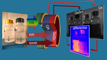
Bottles containing isopropanol and toluene look the same when viewed with the naked eye. A dual-band infrared (IR) detector highlights absorption differences in the near-IR and shortwave-IR, revealing that the bottles hold two different solvents. [Image: Reprinted with permission from E.T. Simola et al., “CMOS-Compatible Bias-Tunable Dual-Band Detector Based on GeSn/Ge/Si Coupled Photodiodes,” ACS Photonics. Copyright 2021 American Chemical Society]
Researchers from Germany and Italy published a design for a silicon-based dual-band infrared detector that can be integrated into existing imaging technologies (ACS Photon., doi: 10.1021/acsphotonics.1c00617). The detector is grown on a silicon wafer using standard manufacturing materials and techniques, resulting in an inexpensive photodiode that can turn a camera into a multimode imager capable of toggling from visible light to near-infrared (NIR) and to shortwave-infrared (SWIR).
“The ability to switch between NIR and SWIR under identical light conditions [and without photoprocessing] gives us access to information that neither band can offer individually,” the authors say. Among the potential applications they see for the dual-band detector are autonomous driving; security, medical, and environmental monitoring; and solid-state spectrometry.
Making IR detection easier
Machine-vision systems and the Internet of Things are pushing the development of optical devices that detect visible, NIR (750–1400 nm) and SWIR (1400–2500 nm) wavelengths. IR spectral ranges reveal details from our environment that are not visible to the naked eye—like air traffic patterns in dense fog and authentication marks on currency.
While most visible-light detectors are silicon-based, IR detectors are typically derived from other materials, complicating their integration into existing imaging systems. This inspired the research team to develop an IR detector grown on a silicon wafer that could be easily added to standard CMOS-compatible imaging processors.
The resulting dual-band detector is a vertical stack of n-i-p-i-n photodiodes fabricated on a 200-mm silicon wafer. The photodiode layers are made of germanium–tin (GeSn) for detecting SWIR, germanium (Ge) for detecting NIR, and silicon (Si) for detecting. The photodiode is tuned to detect NIR or SWIR by reversing the bias voltage applied to the detector.
The researchers characterized their dual-band GeSn/Ge/Si detector performance in room-temperature environments using a tunable laser source.
Characterizing the GeSn/Ge/Si detector
The researchers confirmed the detector’s photoresponse switched from NIR with a negative bias current to SWIR with a positive bias current, with specific detectivities of 1.9×10¹⁰ and 4.0×109 cm-Hz1/2/W, respectively. During these demonstrations, the team found a partial overlap in the two diodes’ photoresponse at 1600 nm that could be overcome by increasing the Ge layer thickness—which is within current industry capabilities—so that it can better absorb radiation at this wavelength.
To test the viability of the detector as a switchable NIR/SWIR imager, the researchers used a 5×5-pixel array to evaluate the amount of optical crosstalk between pixels. Although they observed minimal crosstalk for both NIR and SWIR detection, detector performance could be improved by adding antireflection layers and using a more highly polished silicon wafer. These optimizations were beyond the scope of the current work, but the researchers plan to integrate these changes in future iterations of the detector.
The team conducted additional detector demonstrations that showed its potential use in subsurface examination of paintings, document verification/authentication, absorption-based material identification and integrated solid-state spectrometry.