
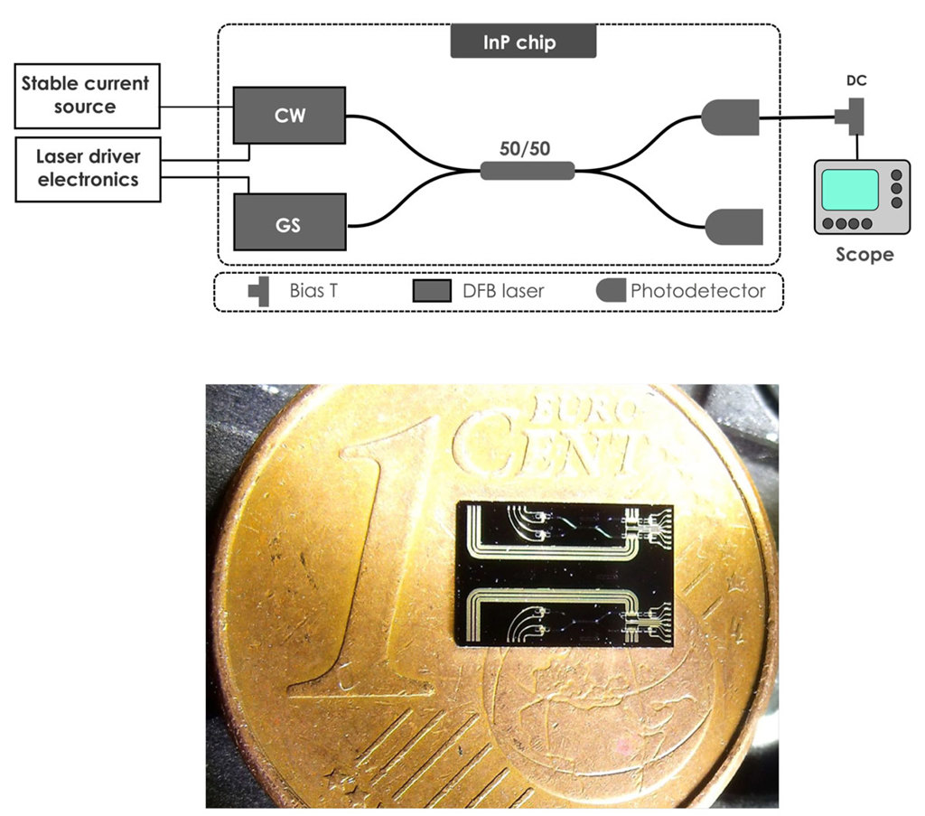
The design by the ICFO-led team consists of an InP chip containing two lasers—one continuous wave, one gain switched—whose beams combine in a multimode interference coupler (top). A photodetector reads the beat from the interfered beams, which is mathematically related to the random phase of pulses from the gain-switched laser, and thus allows random numbers to be rapidly read out. The chip itself is only 6×2 mm in size (bottom). [Image: C. Abellan et al., Optica, doi: 10.1364/OPTICA.3.000989] [Enlarge image]
Online security depends on rapidly generating random numbers, and the faster and more truly random, the better. Scientists from Spain and Italy have now designed an approach that uses that most random of physical processes, quantum mechanics, to churn out random numbers at a rate of gigabits per second—and in a way that can be integrated into existing CMOS chip technology (Optica, doi: 10.1364/OPTICA.3.000989). The combination of speed, true randomness and integration could, according to the team, make the device useful on scales ranging from mobile phones to data centers.
From pseudo to true
Software algorithms are capable of rapidly generating so-called pseudo-random numbers. Because even the best codes are deterministic in nature, however, they are vulnerable to security breaches by determined hackers. A more secure, true random-number generator must be based on a physical process that includes some element of intrinsic randomness; that random element, in turn, is tapped directly and converted into an electrical signal for use in applications.
The phenomena of quantum mechanics—almost a byword for randomness—constitute an obvious candidate for generating high-quality, truly random numbers. But the so-called quantum entropy sources (QESs) that have been developed thus far have tended to require discrete, bulk optical elements, making them a poor fit for driving encryption functions on your cellphone.
Tiny lasers, heterodyne detection
To get to a chip-scale approach for a QES, scientists at several Spanish and Italian institutions, led by OSA Member Valerio Pruneri of the Institute of Photonic Sciences (ICFO) in Barcelona, Spain, took advantage of recent progress with indium phosphide (InP) as a platform for photonic integrated circuits (PICs) that include lasers and other optical components. The team’s new design works by combining the interference of two InP distributed-feedback lasers with heterodyne detection, to allow for rapid harvesting of the random signal generated by the interference.
The team created its prototype QES PIC by using standard fabrication techniques to write two distributed-feedback lasers to an InP chip only 6×2 mm in size. One of the lasers is a continuous-wave source that acts as the local oscillator; the other is operated in a continuously modulated gain-switching mode, which produces pulses with nearly identical waveforms but completely random phases.
Merging the two laser signals in a multimode interference coupler results in an amplitude oscillation whose beat frequency is mathematically related to the (random) phase difference. The beat is picked up by a photodetector, which converts the optical signal into an electrical one. That electrical signal is read at periodic intervals, allowing for a stream of random numbers.
Fast, high-quality randomness
Tests of the prototype showed that it was able to generate random numbers at rates higher than 1 Gbit/s. That’s potentially fast enough for real-time encryption of communications and data streams, as well as for use in computationally intense Monte Carlo simulations and other stochastic applications in science and finance. The researchers also pushed their lab data through autocorrelation tests to measure the quality of the randomness coming from the chip, and found that it stacked up well against that of random numbers generated by much larger, unwieldy QESs built out of bulk components.
The researchers believe that the compatibility of the new device with existing CMOS manufacturing technology makes it a strong candidate for commercial use. “It is a big step forward as far as integration is concerned,” the paper’s lead author, ICFO grad student Carlos Abellan, noted in a press release. Initial applications could target the data center and scientific markets, but, the paper concludes, the technique’s “high level of miniaturization may even make the integration of the QES-PIC device in smartphones and tablets possible.”
