A pattern of UV light, projected on a multimode interference device, created local variations in the refractive index (through plasma dispersion) that allowed the light’s routing through the device to be arbitrarily controlled. [Image: University of Southampton]
A team of scientists in the United Kingdom and France, using a novel setup involving digital micromirror devices (DMDs) and ultrafast femtosecond laser pulses, has demonstrated the ability for all-optical wavefront shaping and control of light flow in silicon photonic integrated circuits (Optica, doi: 10.1364/OPTICA.3.000396). The team lead, Otto Muskens of the University of Southampton (U.K.), believes that the device—analogous to a free-space spatial light modulator—represents “a potentially disruptive new approach” to achieving optically reconfigurable, field-programmable silicon photonic chips.
The need for all-optical control
Externally driven, all-optical control of optical signals has become an increasingly important goal as engineers have eyed ever-shorter length scales for optical links—down to the scale of individual chips. At those tiny length scales, it becomes crucial, in functions such as switching, to avoid the losses and energy costs inherent in transforming the signal between the electronic and optical domains.
While tunable photonic switches and other devices have seen substantial progress in recent years, they have tended to be based on complex, hard-wired device geometries that don’t necessarily offer full control over the on-chip light’s transfer function. To get to a more general approach, Muskens, along with other scientists from Southampton and France’s University of Bordeaux, adapted a common technology, the free-space spatial light modulator, to the silicon photonics domain.
DMD control
The researchers began with a standard silicon-on-insulator multimode interference (MMI) device, a common component of optical circuits used to split and recombine signals. These devices are designed to execute a specific function, with that behavior hardwired into the geometry when the device is fabricated. The Southampton-Bordeaux team wanted to see if it could externally control the flow of light through such a hardwired device in a more general way.
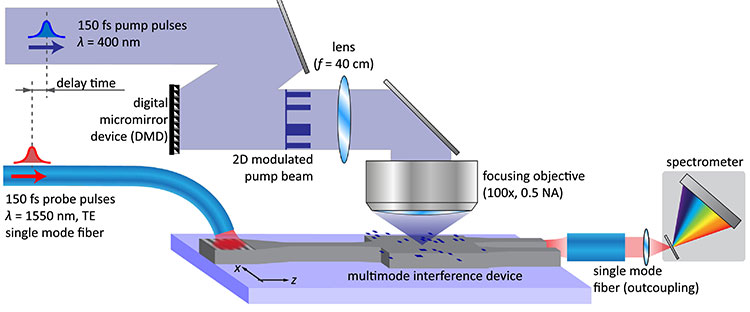
To do so, the scientists sent 150-fs probe pulses at telecom wavelengths (1550 nm) into the integrated MMI device through a single-mode fiber. After a tunable delay time, they pumped 150-fs pulses of ultraviolet (400 nm) light in from above—through an arrangement including a DMD device and a focusing objective—with an eye toward using the UV light to shape the wavefront and control the routing of the probe light in the MMI device:

In the experimental setup, modulation of the external pump light with a digital micromirror device allowed a tunable pattern of UV light—and, thus, of local refractive-index changes—to be projected onto the MMI device. [Image: Bruck et al., Optica, doi: 10.1364/OPTICA.3.000396]
The UV light pulses applied “from the top” temporarily alter the local refractive index in the silicon medium through plasma dispersion, in turn allowing the light flow to be perturbed and redirected optically. The DMD spatially modulates the pump beam to allow for control of the configuration of light projected onto the MMI device surface.
Efficient on-chip routing, negligible loss
The result is the ability to project an arbitrary, and switchable, refractive-index profile onto the MMI device, which in turn sets up all-optical control of the wavefront. Indeed, the team reports that it was able, in a setup involving a 1×2 MMI power splitter, to dynamically route light to any of the output ports with an efficiency of more than 97 percent, and with negligible losses.
The researchers believe that their DMD-based technology could prove useful in designing all-optical, reconfigurable routers, ultrafast modulators, and switches for optical networks. They even see the potential for optical devices that “would provide a similar level of flexibility to the electronic field-programmable gate array”—a potentially significant step toward replacement of electronic components with photonic ones in optoelectronic circuits.

