
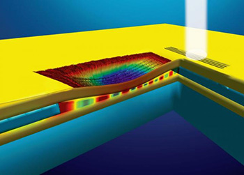
A laser (vertical light) couples to gap plasmons (GPs, alternating red/blue) in a MIM waveguide. A grating matches the laser and GP momentum and the GP propagates through the waveguide depression (rainbow). When the beams are electrically actuated towards the bottom MIM layer, the refractive index increases, phase-retarding the GP. Credit: Brian Dennis, Rutgers University
Advances in confining optical energy within plasmonic devices are helping to further miniaturize photonics, which may lead to on-chip switching and reconfigurable optical circuits. But for mode sizes approaching 10 nm, there’s a significant loss of energy into the metal of the device. U.S. researchers from Rutgers University and the National Institute of Standards and Technology report using a nanoelectrochemical phase-modulation principle to overcome this compression bottleneck (Nat. Photon., doi: 10.1038/NPHOTON.2015.40). After demonstrating optical modulation of a signal in a 200-nm-high waveguide, the team proposed placing this modulator next to a similar static device to create a 2x2 switch. They also numerically showed that their compact modulators could be scaled down to the size of electronic devices.
The research team designed and experimentally demonstrated a gap plasmon phase modulator (GPPM) with a metal-insulator-metal (MIM) structure—in this case, gold-air-gold--taking advantage of the dependence of MIM gap plasmon phase velocity on variable gap size. The modulation occurs when a force generated by the device deforms the top gold layer of the MIM. The researchers were able to implement a 23-micron-long waveguide with a 200-nm gap range using the technique. And, based on previous research, they propose that when one of these modulators is placed next to a static device it would act as a 2x2 optical switch. With computer modeling, they showed that their waveguide could be scaled down to just 1 micron with a 20-nm gap range, without a significant loss of energy.
The 2x2 optical switch could prove useful for electrically tunable plasmonic devices. The new sub-micron optical switch technology could “enable a new class” of on-chip optical switch fabrics and reconfigurable plasmonic optics, according to the scientists.