
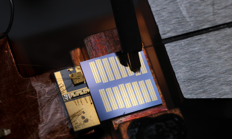
 Lithium tantalate has been used to create an electro-optic frequency comb with a spectral range greater than 60 THz, around four times wider than can be achieved with lithium niobate. [EPFL]
Silicon photonics has been a crucial catalyst for the information revolution, allowing data-rich optical signals to be routed and manipulated within a wafer-scale platform that can be manufactured at scale. Combining multiple components within a densely integrated photonic chip has yielded pluggable devices that can send, receive and process optical information, allowing short fiber links to replace electrical connections within data centers. Such all-optical processing can boost speeds and reduce power consumption, both of which are critical requirements to support the rise of real-time applications such as cloud computing, artificial intelligence and multiplayer online gaming.
But the capabilities of silicon-based devices are struggling to keep pace with the relentless demands of the hyperscalers. While optical transceivers operating at speeds of 100 Gbit/s have been widely installed, modern data centers are driving a shift to data rates of 400 or 800 Gbit/s. Transceivers operating in the terabit regime are now starting to emerge, with the current trajectory suggesting that optical modules will need to deliver 3.2 Tbit/s before the end of the decade.
The biggest bottleneck for silicon will be to transfer digital information into the optical domain at such high data rates. Today’s silicon modulators typically operate at speeds of up to 50 Gbit/s, with ongoing research aiming to push the limit toward 100 Gbit/s. On-chip multiplexing has so far enabled transceiver modules to support faster data rates, with silicon photonics providing the dense integration needed to implement multiple channels for parallel processing. But extending these schemes beyond four or eight channels will be challenging, prompting researchers to investigate alternative platforms that could provide faster modulation speeds within a compact form factor.
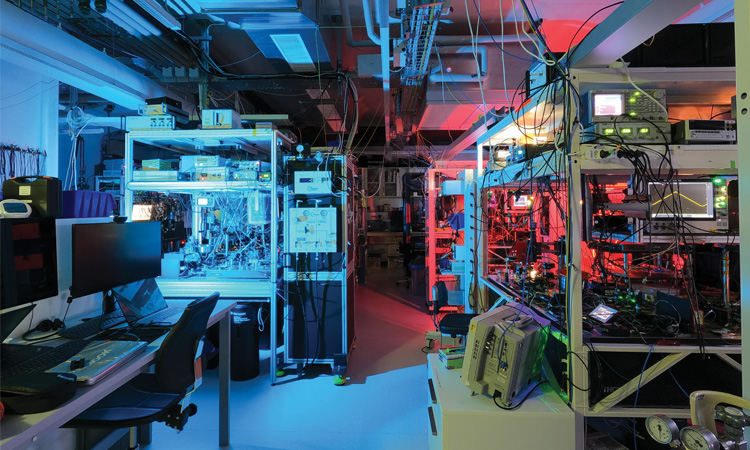 The photonics laboratory at the Swiss Federal Institute of Technology Lausanne (EPFL). [EPFL]
Material matters
The fundamental problem for silicon is that electrical signals do not elicit an intrinsic optical response from the material. Instead, an indirect response must be engineered by exploiting its semiconducting properties to alter the density of charge carriers close to a p–n junction. This change in carrier concentration induces a local variation in the refractive index that modulates the phase of the optical beam, and interferometric techniques are then used to convert these phase shifts into intensity changes that are easier to detect.
However, the reliance on moving around charge carriers slows down the response time. The free carriers also absorb light, with the optical losses increasing when the silicon is more heavily doped to boost the modulation speed and increase the change in refractive index that can be achieved within an acceptable power envelope.
This inherent trade-off between the speed and power efficiency of silicon modulators has motivated researchers to explore alternative materials for high-speed optical transceivers. Prime among them has been lithium niobate, which for decades has been the optical material of choice for the bulk modulators used in long-haul communications networks. Its appeal stems from lithium niobate’s strong electro-optic effect, which causes its refractive index to change in response to an electric field. Importantly, this innate behavior is almost instantaneous, eliminating any fundamental barriers to achieving high modulation speeds. The strength of the electro-optic effect in lithium niobate also generates large phase shifts at low voltages, while its linear dependence on the electric field delivers the precise and predictable phase shifts needed to support coherent transmission and advanced modulation formats.
Exploiting the so-called “smart-cut” process, researchers created wafers of lithium niobate topped with a slice of single-crystal material less than one micrometer thick.
But it was not until the late 2000s that lithium niobate became a viable proposition for integrated photonics. Exploiting the so-called “smart-cut” process that had previously enabled thin layers of silicon to be cut and bonded to an insulating substrate, researchers created wafers of lithium niobate topped with a slice of single-crystal material less than one micrometer thick. This uppermost layer is bonded to a cladding layer of silica, which provides the contrast in refractive index needed to confine light within the electro-optic material.
The commercial availability of these high-quality wafers, initially through Chinese company NanoLN, prompted researchers to fabricate chip-scale modulators within this lithium-niobate-on-insulator (LNOI) platform. In a landmark result in 2018, Marko Lončar’s team at Harvard University, USA, exploited LNOI technology to demonstrate a modulator that supports data rates of up to 210 Gbit/s while being driven by standard on-chip electronics. The device also consumed much less power than silicon equivalents, confirming lithium niobate as the favored option for next-generation optical modulators.
This result triggered a period of rapid innovation, with researchers pushing the performance of LNOI modulators and demonstrating many of the other devices that are needed for an integrated photonics platform. But commercial adoption of the technology has been slowed by the lack of investment into scalable manufacturing processes, and commercial LNOI wafers remain limited in size and expensive to produce.
To achieve the scalability and cost control needed for high-volume datacom applications, researchers have instead devised various strategies to integrate modulators made from thin-film lithium niobate into silicon-based devices. “The most practical solution is to add extra capabilities into the mature manufacturing processes we already have for silicon photonics,” says Maximilien Billet of the University of Ghent and imec, a leading innovation hub for microelectronics in Leuven, Belgium. “We have used heterogeneous integration to incorporate other optical technologies onto silicon wafers, such as laser sources and high-speed photodetectors, and for electro-optic modulators we can achieve a similar performance while still accessing the scale and functionality of the silicon platform.”
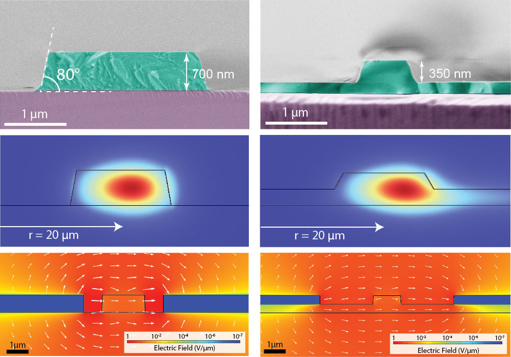 [Enlarge image]The fabrication technique developed by researchers at EPFL exploits a mask of diamond-like carbon to create fully etched waveguides (left) that are thicker and have steeper sidewalls than ridge waveguides (right). These strip waveguides confine light more tightly without introducing losses at the electrodes. [EPFL]
Rediscovered potential
However, a continued focus on reducing the footprint of lithium niobate devices has revealed some niggling issues with using the platform for tightly integrated components. In 2023, Tobias Kippenberg and his team at the Swiss Federal Institute of Technology Lausanne (EPFL) devised a fabrication process that exploits a mask of diamond-like carbon (DLC) to create fully etched “strip” waveguides in LNOI wafers. These strip waveguides confine light more tightly than the ridge-shaped structures that had previously been the norm, making it possible to increase the circuit density while maintaining ultralow losses. However, the Swiss researchers ran into a problem.
“Lithium niobate has a large birefringence, which means that the refractive index depends on the direction the light is propagating relative to the orientation of the crystal,” Kippenberg explains. “That made it difficult to design complex photonic circuits that require tight bends, such as microresonators or arrayed waveguide gratings [AWGs] for multiplexing.”
The birefringence of lithium niobate splits light into two optical beams with opposite polarizations, each of which travels at different speeds through the crystal. In bulk modulators this directional dependence is an asset, since the crystal can be cut to isolate the polarization that generates the strongest electro-optic response. In microstructured waveguides, however, the speed of the two different polarizations changes whenever light travels around a bend. As they cross over, unwanted coupling between the two polarization modes makes it difficult to achieve the accurate phase control needed for precise and reliable modulation.
At the same time, Kippenberg was wondering whether other materials could benefit from the deep-etching DLC technology they had developed for lithium niobate. “While reading the literature we came across lithium tantalate, which for decades has been used commercially for the acoustic filters in mobile phones,” he explains. “When we looked into its optical properties, we found that lithium tantalate produces almost the same electro-optical response as lithium niobate while also having a lower birefringence.”
Lithium tantalate has a more stable crystal structure than lithium niobate, which makes it more resilient to optical damage for applications requiring high-power modulation.
Other advantages emerged. Lithium tantalate has a more stable crystal structure than lithium niobate, which makes it more resilient to optical damage for applications requiring high-power modulation. It is also less sensitive to temperature and less prone to drift, enabling devices to maintain a consistent output over time. With a slightly wider transparency window, lithium tantalate can also extend the available operating regime into the deep ultraviolet.
However, lithium tantalate had not previously been considered for integrated photonic circuits, mainly for historical reasons. The first bulk modulators were fabricated by diffusing titanium into the material, but the high temperatures needed for this process cause lithium tantalate to lose its electro-optic properties. By the time thin-film technologies had enabled structures to be directly etched into the material, researchers were locked into lithium niobate as the best choice for integrated photonics. “The community had largely forgotten about the excellent optical properties of lithium tantalate, and it remained primarily associated with acoustic devices,” comments Kippenberg.
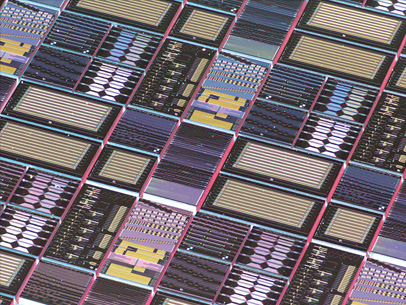
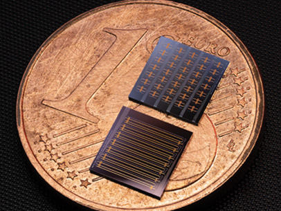 Lithium tantalate provides a scalable platform for fabricating integrated photonic chips. [EPFL]
A tale of two materials
Lithium tantalate and lithium niobate are chemical and structural analogs that share many of the same properties. They both have crystal lattices that lack a center of inversion, generating an offset between the positions of the charged ions along one of the axes. This imbalance in the charge distribution makes them both ferroelectric, possessing a natural polarization that can be switched by an electric field.
Reversing the polarization has a direct effect on the refractive index of the crystal, resulting in a strong electro-optic effect that depends linearly on the electric field. Both materials are also piezoelectric, an attribute that has been widely exploited for acoustic devices, and they exhibit higher-order nonlinear effects that have been harnessed for applications such as second-harmonic generation.
However, lithium tantalate is stronger and more stable than lithium niobate. It has a wider bandgap and a crystal structure that contains fewer defects, which makes it more resistant to optical damage at high pump powers. This enhanced stability also reduces the chance of light–matter interactions that cause the operating point of devices to drift.
In contrast, lithium niobate is susceptible to the photorefractive effect, in which photons absorbed by the material are able to excite electrons occupying defect energy states inside the bandgap. When these electrons migrate and become trapped elsewhere, they create an internal electric field that adds a slowly changing component to the optical response.
This effect is exacerbated by the higher photon energies at visible wavelengths, which makes lithium tantalate an attractive option for applications in this regime. Its wider bandgap also extends the transparency window into the deep ultraviolet, offering the potential of frequency conversion between ultraviolet and visible wavelengths.
Meanwhile, the use of lithium tantalate within mobile phones had enabled the evolution of a mature manufacturing technology. Kippenberg discovered that wafers of lithium-tantalate-on-insulator (LTOI) were already being produced commercially, potentially offering greater economies of scale than the lithium niobate platform. “The cost of the wafers is not really driven by the demand in photonics, where the demand is small when compared with microelectronics,” he says. “Having a volume application like acoustic filters for phones can drive down the cost of the substrate, which suggested to me that LTOI could provide a commercially viable platform for integrated photonics.”
Into the light
Having rediscovered the potential of lithium tantalate, Kippenberg and his team started a systematic investigation of its capabilities for chip-scale photonic devices. They collaborated with Xin Ou and colleagues at the Shanghai Institute of Microsystem and Information Technology in China, who used the smart-cut process to fabricate optical-grade LTOI wafers with lower defects and more uniform layers than those manufactured for radio-frequency applications. This customized fabrication process allowed the researchers to optimize the material stack and the thickness of the oxide layers, enabling them to adapt the deep-etching technology to the LTOI platform.
In 2024, Kippenberg and his collaborators showed that tightly confining waveguides could be fabricated in lithium tantalate with losses of less than 6 dB/m, lower than can be achieved with standard silicon photonics and approaching the performance offered by state-of-the-art devices made from silicon nitride. They also confirmed that thin-film lithium tantalate delivers the same electro-optic performance as lithium niobate, with a birefringence around 17 times lower at telecom wavelengths.
Later the same year, the team demonstrated a modulator in the LTOI platform that achieved the ultrahigh bandwidth needed for next-generation datacomms. When combined with high-density data transmission protocols, this LTOI modulator could encode optical information at speeds of more than 400 Gbit/s. What’s more, the optical power produced by the device drifted by just 3 dB, compared with around 8 dB for lithium niobate, avoiding the need for mitigating strategies that consume more power and add complexity to the circuit design.
While these initial results were obtained using a bespoke LTOI process, Kippenberg’s group has since found that the same performance advantages can be realized using commercial acoustic-grade wafers. “As we explored the platform further, we were impressed by how lithium tantalate addressed many of the challenges we had faced with lithium niobate,” he says. “It seemed to me that lithium tantalate is a wonder material that could enable the scalable manufacture of photonic integrated circuits that support multiple functionalities.”
These impressive results have reignited interest in lithium tantalate as a photonic platform. In quick succession, other groups demonstrated high-speed modulators and optical switches in the material, confirming that these devices deliver lower losses and greater stability than those made from lithium niobate. The low birefringence of lithium tantalate has also enabled Kippenberg’s group to fabricate low-loss AWGs, while Daoxin Dai and colleagues at Zhejiang University in China have used the LTOI platform to demonstrate an integrated transmitter that combines electro-optic modulators with an eight-channel AWG for wavelength-division multiplexing.
Meanwhile, Billet and his team have demonstrated that a lithium tantalate modulator can be integrated with imec’s established process technology for silicon photonics. Exploiting the same techniques that were previously used for lithium niobate, the prototype modulator delivers a bandwidth of 70 GHz and data rates of more than 320 Gbit/s when combined with pulse-amplitude modulation. “It is useful to show that heterogeneous integration is possible with lithium tantalate, even though its material properties are slightly different,” says Billet. “For this sample demonstration, the performance was close to what can be achieved on native wafers.”
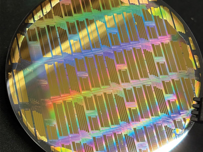
 Photonic integrated circuits fabricated by Luxtelligence on a lithium tantalate wafer. [Luxtelligence]
Industrial development has also followed. For example, Swiss startup Luxtelligence, initially formed to commercialize the deep-etching technology developed by Kippenberg and his team for lithium niobate, now offers a foundry service for lithium tantalate devices. “We are building a new integrated photonics architecture that exploits lithium tantalate’s mature wafer manufacturing technology and superior optical properties,” says Alberto Beccari, the company’s chief technology officer.
Companies producing LTOI wafers have also adapted their processes to meet the needs of emerging optical applications. “When we started our company, we could buy 100-mm wafers produced to acoustic-level quality,” says George Li, cofounder of Lumina Corp., a US–Australian startup that has the scientific backing of Marko Lončar. “Now we can source optical-grade wafers in sizes up to 150 mm, with 200-mm versions likely to become available within the next year or two.”
Open to ideas
However, Li remains skeptical that the performance benefits of lithium tantalate will be enough to displace incumbent technologies for high-volume applications. “We see a lot of resistance from hyperscalers and data centers to shift from silicon photonics,” says Li. “Lithium tantalate is a better material than niobate at telecom wavelengths, but it’s not so much better than silicon photonics to compete in that market.”
Instead, Lumina sees a larger opportunity in developing chip-scale modulators that operate in the visible regime. Manipulating light at these wavelengths, which is particularly important for applications in biomedicine, microscopy and quantum control, currently requires free-space optical solutions that increase the size and power requirements of the system. More compact modulators could enable the development of portable medical devices and wearable biosensors, as well as high-speed control systems for manipulating the qubits in atom-based sensors and quantum computers. “Lithium tantalate is very good at visible wavelengths,” says Li. “As far as I’m aware, there are no other platforms that can produce integrated electro-optic modulators in this spectral range, particularly for blue light and into the ultraviolet.”
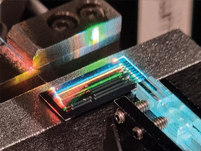 Startup Lumina is developing integrated modulators made from lithium tantalate that deliver low-loss performance at visible wavelengths. [Lumina]
Although existing tools and techniques have provided a useful starting point for the Lumina team, operating at shorter wavelengths requires smaller components that place extra constraints on the fabrication process. Over the last two years, they have been working to reconfigure the process parameters to produce devices that deliver high-speed performance in this regime. “We are pioneering chip-scale integration at these wavelengths,” says Li. “At shorter wavelengths we’re still working to get the loss down, but we now have a relatively mature process that is producing the quality we need.”
Kippenberg and his team are also exploring applications that extract more value from lithium tantalate’s unique material properties. As an example, they have demonstrated an electro-optic frequency comb that provides more than 2,000 distinct lines over a frequency range greater than 60 THz. Such electro-optic devices offer an attractive alternative to other chip-scale solutions, since they provide greater stability and more flexible operating parameters, but the spectral range of frequency combs based on lithium niobate are limited by mode mixing at high frequencies.
The lower birefringence of lithium tantalate overcomes this problem, extending the available frequency span by a factor of four. The design of this comb also showcased the potential of LTOI to provide a unified platform for integrating electro-optic devices with the microwave circuits that drive their response. While previous combs made from lithium niobate have required large microwave powers, this integrated approach enhanced the electro-optic coupling to reduce the on-chip power consumption, improve the stability of the output, and shrink the footprint of the comb generator to just 1 cm2.
 Kippenberg’s group has shown that industry-standard processes for fabricating high-density copper interconnects can be combined with the LTOI platform. [EPFL]
Achieving such tight integration between microwave and electro-optic devices could deliver improved outcomes across multiple applications, including chip-scale optical metrology, control systems for superconducting qubits, and hybrid processors that create and control microwave signals in the optical domain. One possibility that Kippenberg and his team have already explored is the potential of the lithium tantalate platform to outperform the electronic receivers currently being used in wireless communications systems.
“These receiver front-ends are now being pushed into the terahertz regime, but the noise performance of the transistors rapidly degrades at these frequencies,” he explains. “By integrating an electro-optical modulator made from lithium tantalate with a millimeter-wave cavity, we have created an integrated optical receiver that can surpass the performance of state-of-the-art electronic solutions for next-generation wireless networks.”
LTOI offers a compelling alternative in application domains that can benefit from its higher electro-optic bandwidth and lower switching voltage.
This application benefits from the unique capability of lithium tantalate to handle high powers, but such efficient coupling will also be essential for emerging data-center applications that require the optical transceiver and processing chip to be integrated into the same package. In a step toward that goal, Kippenberg’s group has shown that the lithium tantalate platform can support industry-standard processes for fabricating high-density electrical connections from copper. These electrodes reduce the on-chip microwave losses by as much as 10%, allowing the team to demonstrate a modulator that can operate at speeds of up to 540 Gbit/s when used with an eight-level transmission protocol.
“LTOI-based optical chips are unlikely to replace silicon photonics for cost-sensitive applications where dense integration of passive components is the primary requirement,” says Kippenberg. “However, LTOI offers a compelling alternative in application domains that can benefit from its higher electro-optic bandwidth and lower switching voltage, particularly coherent optical communications and interconnects that require high-speed and low-power modulation.”
Susan Curtis is a freelance science and technology writer based in Bristol, UK.
References and Resources
-
C. Wang et al. “Integrated lithium niobate electro-optic modulators operating at CMOS-compatible voltages,” Nature 562, 101 (2018).
-
C. Wang et al. “Lithium tantalate photonic integrated circuits for volume manufacturing,” Nature 629, 784 (2024).
-
C. Wang et al. “Ultrabroadband thin-film lithium tantalate modulator for high-speed communications,” Optica 11, 1614 (2024).
