
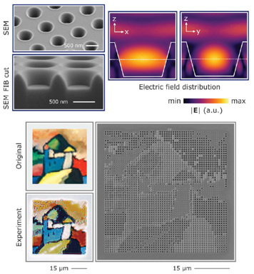
 [Enlarge image]Top: SEM images of experimentally realized Mie voids created by focused ion beam milling into silicon, with simulated electric-field distribution of the lowest-order mode, highlighting the confinement in air. Bottom: Nanoscale color printing with Mie voids at a resolution of 36,000 dots per inch. Each pixel is composed of one void with a specific depth and diameter.
Manipulating, controlling and utilizing the flow of light at surfaces and interfaces has been an important challenge. Nanophotonics has greatly aided these efforts, enabling a plethora of novel optical devices including metalenses, beam-shaping devices, optical sensors, quantum emitter–antenna coupling schemes and nanoscale color generators. These devices use individual resonant building blocks that allow manipulation of the phase and amplitude of scattered light using dielectrics (such as Mie-tronics1) or plasmonic excitations.
Confinement of light inside metallic and dielectric materials constitutes a significant drawback, however. The resonant modes are subject to both loss and dispersion of the materials, limiting the working range. Moreover, for dielectric systems, the largest part of the modal field is inaccessible inside the material, limiting nanoscale sensing and nanoscale coupling.
Recently, we introduced a different approach that can overcome these limitations: resonant light confinement in air.2 We revealed that a void created in a high-index material supports localized resonant modes. We named such structures Mie voids, in close analogy to the well-known Mie modes of high-index resonators. Intuitively, both systems rely on Fresnel reflection at the interface of higher- and lower-index materials as the basic working mechanism.
Despite the close analogy, there is one paramount difference: Mie voids resonantly confine light in air rather than inside a high-index host material, which allows confinement of radiation even in wavelength regions of significant host-material absorption. We experimentally demonstrated resonant confinement of UV radiation down to 265 nm or 4.68 eV in a silicon. What is more, the entire modal volume is accessible. These properties make Mie voids an ideal platform for optical sensing as well as for coupling the resonant modes to (for example) emitters or molecular excitations.
While these results have profound implications, the color generated by the voids is visually the most fascinating aspect. The optical response of the individual voids, tunable over the entire visible wavelength range, results in spectral features of ideal linewidth for brilliant, intense and naturalistic colors. Mie voids are therefore excellent candidates for nanoscale color printing at the highest resolution.
We believe that Mie voids offer unique properties that will aid many areas of nanophotonics. They will push the operation of functional high-index metasurfaces into the blue and UV spectral range. This extension, in turn, should enable novel antenna and structure designs that will benefit from full access to the modal field inside the void as well as a nearly free choice of the high-index material for novel sensing and active-manipulation strategies.
Researchers
Mario Hentschel and Harald Giessen, University of Stuttgart, Stuttgart, Germany
Kirill Koshelev and Yuri Kivshar, Australian National University, Canberra, Australia
Thomas Weiss, University of Graz, Graz, Austria
References
1. Y. Kivshar. Nano Lett. 22, 3513 (2022).
2. M. Hentschel et al. Light Sci. Appl. 12, 3 (2023).
