
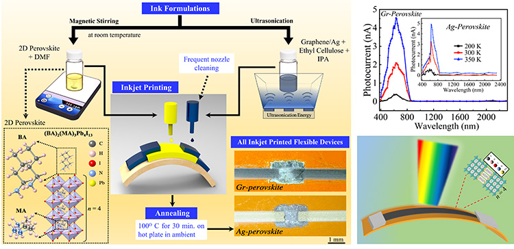
 Left: Process flow for a 2D-perovskite-based photodetector. Top right: The photodetector’s wavelength-dependent photocurrent response. Bottom right: Schematic of the 2D photodetector under illumination on a flexible substrate, during which the 2D absorber remained photoresponsive under mechanical strain.
The strong light–matter interactions in absorbers made with 3D organic–inorganic perovskites has catapulted the photovoltaics community to achieving high power conversion efficiencies in solar cells, as well as toward other optoelectronic platforms such as photodetectors for optical communication, environmental monitoring and space exploration. This year, we expanded the manufacturing and application space for these important materials by demonstrating a method for ink-jet printing of 2D perovskites, along with the electrical contacts, on flexible substrates.1
Breakthroughs in 3D perovskites toward their strong light–matter interactions were first reported less than a decade ago, with methyl-ammonium lead triiodide (MAPbI3, CH3NH3PbI3) being one of the most widely studied perovskite compositions.2 Although the high optical absorption efficiency of 3D perovskites has captured the spotlight, their main drawback is instability in the presence of moisture. The recent family of direct-band-gap 2D layered perovskites, with the formula (CH3(CH2)3NH3)2(CH3NH3)n-1PbnI3n+1, offers more optical tunability through compositional variation, and are environmentally more stable, where the alkyl ammonium layer deters water molecules to enhance moisture resistivity.3
The synthesis of 2D perovskite crystals relies on solution processes and vapor-phase conversion, but little work has been done on forming 2D perovskite photodetectors with ink-jet printing on flexible substrates. Additionally, one of the key parameters for achieving optimal device performance for optical-to-electrical transduction lies in the ability to control charge carrier flow, so contact engineering with the perovskite plays a key role for charge collection.
In our recent work, we demonstrated ink-jet-printed 2D perovskite for photodetectors on flexible substrates. We used this all-additively-manufactured approach to print not only the 2D perovskite absorber, but also the electrical contacts with graphene (Gr) and silver (Ag) inks for efficient charge collection.1
From the temperature-dependent transport with both Gr and Ag contacts, we were able to correlate the photoresponse to the Schottky barrier at the interfaces,1 and the structural phase transitions in the 2D perovksites.4 The wavelength-dependent photocurrent from the visible-to-IR peaked at ~630 nm, consistent with the band gap of our absorber.1,5 We also conducted strain-dependent optomechanical tests under illumination, where the photocurrent decreased with increasing strain.
Our findings validate the importance of 2D perovskites with inkjet-printed contacts, and the figures of merit obtained suggest that our solution-processed absorbers are well positioned to impact future research in flexible optoelectronics and photovoltaics using scalable additive-manufacturing routes.
Researchers
M. Sharma, R.F. Hossain and A.B. Kaul, University of North Texas, Denton, TX, USA
References
1. R.F. Hossain et al. npj 2D Mater. Appl. 5, 34 (2021).
2. M.M. Lee et al. Science 338, 643 (2012).
3. D.H. Cao et al. J. Am. Chem. Soc. 137, 7843 (2015).
4. M. Min et al. ACS Appl. Mater. Interf. 12, 10809 (2020).
5. M. Sharma et al. IEEE Intl. Flexible Electronics Tech. Conf. (IFETC 2021).
